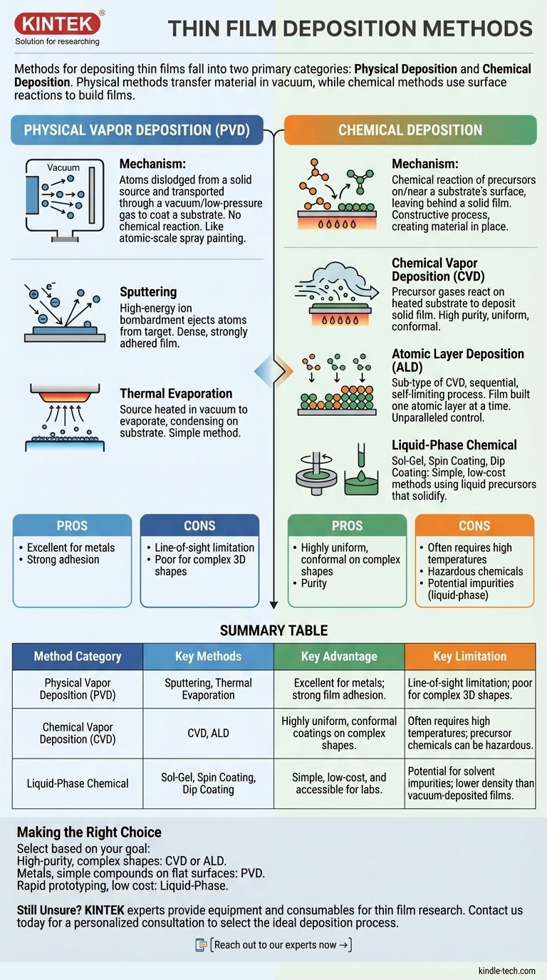
The primary methods for depositing thin films fall into two main categories: Physical Deposition and Chemical Deposition. Physical methods, such as sputtering and thermal evaporation, involve physically transferring material from a source to a substrate, often in a vacuum. Chemical methods, including chemical vapor deposition (CVD) and sol-gel techniques, use chemical reactions on a surface to build the film layer by layer.
The choice between physical and chemical deposition is not about which is "better," but which process offers the right control, material compatibility, and scalability for your specific goal. Physical methods essentially "move" existing atoms, while chemical methods "build" the film from chemical precursors.
The Two Pillars of Deposition: Physical vs. Chemical
To select the right technique, you must first understand the fundamental difference in how these two families of methods operate.
What is Physical Vapor Deposition (PVD)?
Physical Vapor Deposition encompasses methods where atoms are dislodged from a solid source material and transported through a vacuum or low-pressure gas to coat a substrate.
There is no chemical reaction involved in forming the film itself. Think of it as an atomic-scale spray painting process, where tiny particles of the "paint" (the source material) travel directly to the surface you want to coat.
What is Chemical Deposition?
Chemical Deposition methods involve the reaction of chemical precursors on or near a substrate's surface, leaving behind a solid film.
This process is fundamentally constructive. Instead of just moving material, you are creating it in place through a controlled chemical transformation. An analogy is steam (the precursor) condensing and freezing on a cold window (the substrate) to form a uniform layer of ice (the film).
A Closer Look at Physical Deposition Methods
PVD techniques are workhorses of industry, particularly for metals and simple ceramic compounds.
Sputtering
In sputtering, a target made of the desired film material is bombarded with high-energy ions (typically from an inert gas like argon) within a vacuum chamber.
This bombardment acts like an atomic-scale sandblaster, knocking atoms off the target. These ejected atoms then travel and deposit onto the substrate, forming a dense and strongly adhered film.
Thermal Evaporation
This is one of the simplest PVD methods. The source material is heated in a high vacuum until it evaporates, turning into a gas.
This vapor then travels in a straight, line-of-sight path and condenses on a cooler substrate, much like water vapor condenses on a cold glass. Variations like electron beam evaporation use a focused electron beam to heat the material.
A Closer Look at Chemical Deposition Methods
Chemical methods offer unique advantages, especially for creating highly pure, uniform films over complex surfaces.
Chemical Vapor Deposition (CVD)
In CVD, precursor gases are introduced into a reaction chamber containing a heated substrate. The heat triggers a chemical reaction, causing a solid material to deposit on the substrate.
CVD is renowned for creating exceptionally pure and uniform (conformal) coatings that can cover even complex, three-dimensional shapes evenly. Plasma-Enhanced CVD (PECVD) is a variant that uses plasma to enable these reactions at lower temperatures.
Atomic Layer Deposition (ALD)
ALD is a sub-type of CVD that offers the ultimate in precision. It works by introducing precursor gases one at a time in a sequential, self-limiting process.
This allows you to build a film quite literally one single atomic layer at a time, providing unparalleled control over thickness and composition.
Sol-Gel, Spin Coating, and Dip Coating
These are liquid-phase chemical methods that are often simpler and less expensive than vacuum-based techniques.
Spin coating involves dispensing a liquid precursor onto a substrate and spinning it at high speed to create a thin, uniform layer. Sol-gel and dip coating involve applying a liquid chemical solution that solidifies into a film upon drying or heating.
Understanding the Trade-offs
No single method is perfect for every application. The limitations of each approach are critical to your decision.
PVD: Line-of-Sight Limitations
Because atoms in PVD travel in a straight line from the source, it can be difficult to uniformly coat the "shadowed" areas of complex, 3D objects. This is a significant drawback for non-flat substrates.
CVD: Temperature and Chemistry Constraints
Traditional CVD often requires very high substrate temperatures, which can damage sensitive materials like polymers or certain electronics. The precursor chemicals can also be highly toxic, corrosive, or expensive.
Liquid-Phase: Simplicity vs. Purity
While simple and low-cost, methods like spin coating can introduce impurities from solvents into the final film. They also may not achieve the same density or adhesion as films produced in a vacuum environment.
Making the Right Choice for Your Goal
Selecting a method requires matching the process capabilities to your desired outcome.
- If your primary focus is high-purity, uniform coating on complex shapes: CVD or ALD are often the superior choice due to their chemical reaction-based, conformal nature.
- If your primary focus is depositing metals or simple compounds onto flat surfaces: PVD methods like sputtering and evaporation are highly effective, reliable, and widely used in industry.
- If your primary focus is rapid prototyping or low-cost application: Liquid-phase methods like spin coating or sol-gel provide an accessible and straightforward solution, especially in a lab setting.
Ultimately, understanding the fundamental mechanism of each method is the key to selecting the right deposition technique for your objective.
Summary Table:
| Method Category | Key Methods | Primary Mechanism | Key Advantage | Key Limitation |
|---|---|---|---|---|
| Physical Vapor Deposition (PVD) | Sputtering, Thermal Evaporation | Physically moving atoms from a source to a substrate in a vacuum. | Excellent for metals; strong film adhesion. | Line-of-sight limitation; poor for complex 3D shapes. |
| Chemical Vapor Deposition (CVD) | CVD, ALD (Atomic Layer Deposition) | Chemical reaction of precursors on the substrate surface. | Highly uniform, conformal coatings on complex shapes. | Often requires high temperatures; precursor chemicals can be hazardous. |
| Liquid-Phase Chemical | Sol-Gel, Spin Coating, Dip Coating | Application of a liquid precursor that solidifies into a film. | Simple, low-cost, and accessible for labs. | Potential for solvent impurities; lower density than vacuum-deposited films. |
Still Unsure Which Thin Film Deposition Method is Right for Your Project?
Choosing the right technique is critical for achieving the desired film properties, whether you need high purity, uniform coverage on complex shapes, or a cost-effective lab solution. The experts at KINTEK are here to help.
We provide the equipment and consumables to support your thin film research and production, including systems for sputtering (PVD), CVD, and more.
Contact our team today for a personalized consultation. We'll help you select the ideal deposition process to meet your specific material, performance, and budget goals.
Reach out to our experts now →
Visual Guide