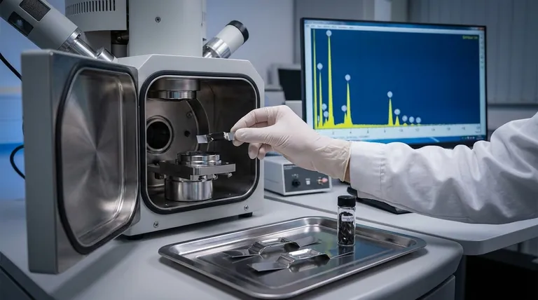
The primary reason for using carbon coating in SEM is for elemental analysis, specifically Energy Dispersive X-ray Spectroscopy (EDX or EDS). While other metal coatings are better for imaging, carbon's unique properties ensure that it does not interfere with or obscure the X-ray signals emitted from the elements within your actual sample.
The choice of a coating material for SEM is a critical decision driven by your ultimate goal. Highly conductive metals like gold are used to get the best possible image, while carbon is used to get the most accurate elemental data.
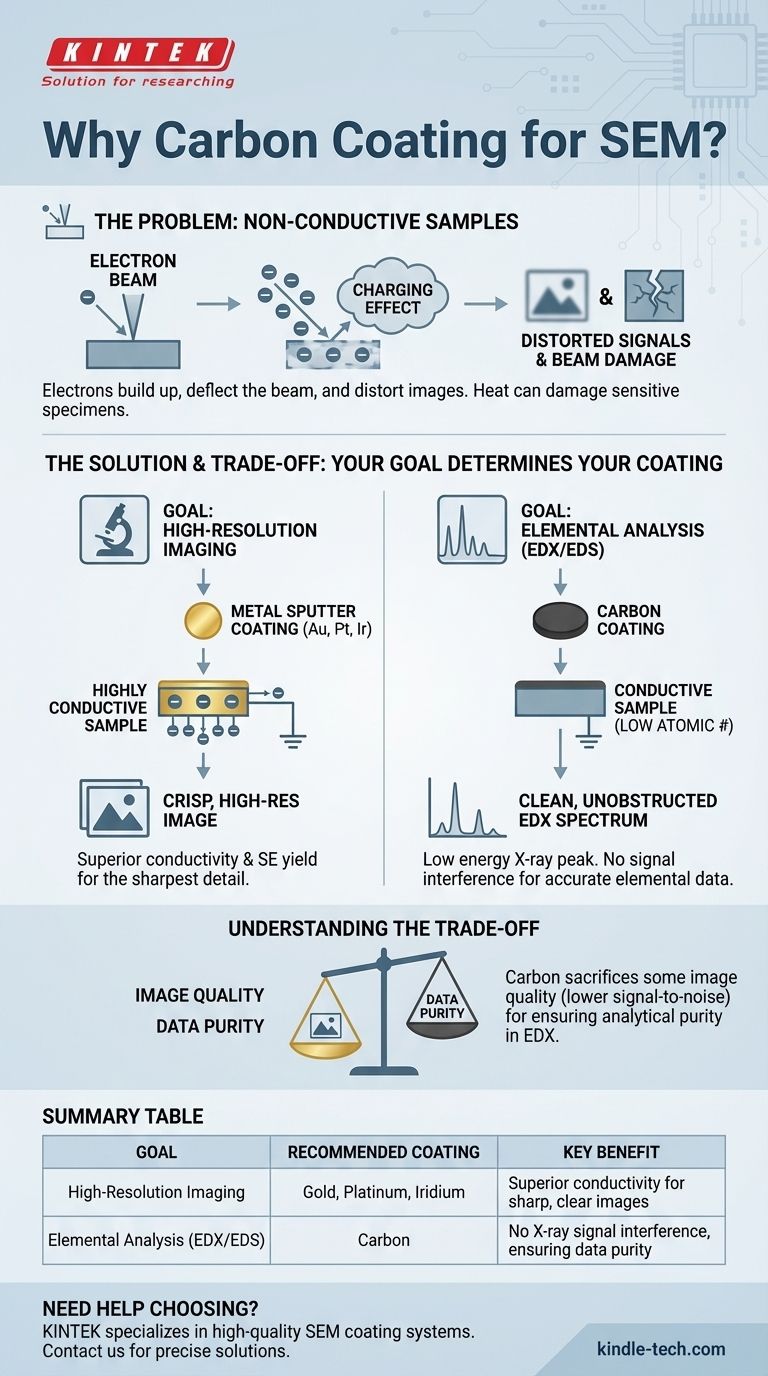
The Fundamental Problem: Non-Conductive Samples
Scanning Electron Microscopy works by scanning a focused beam of electrons over a surface. For this process to work correctly, the sample must be conductive. Many biological or geological specimens are not.
The "Charging" Effect
When the electron beam hits a non-conductive (insulating) surface, the electrons have nowhere to go. They accumulate on the surface, creating a negative charge.
This "charging" effect deflects the incoming electron beam and distorts the emitted signals, resulting in bright patches, streaks, and a loss of image detail. A conductive coating provides a path for these excess electrons to drain away to the ground.
Poor Signal and Beam Damage
Insulating materials are often poor emitters of the secondary electrons (SE) needed to form a high-quality image. This results in a low signal-to-noise ratio and a blurry or grainy final image.
Furthermore, the focused energy of the electron beam can heat up and damage sensitive samples. A conductive coating helps dissipate this heat and electrical charge, protecting the specimen.
Your Goal Determines Your Coating
The coating you choose is a direct trade-off between maximizing image quality and ensuring analytical accuracy.
For High-Resolution Imaging: Use Metals
If your only goal is to get the sharpest, clearest image possible, a metal sputter coating like gold (Au), platinum (Pt), or iridium (Ir) is the superior choice.
These metals are excellent electrical conductors and have a high secondary electron yield. This means they effectively prevent charging and generate a strong, clear signal for the detector, resulting in crisp, high-resolution images.
For Elemental Analysis (EDX/EDS): Use Carbon
If you need to determine the elemental composition of your sample using EDX, a metal coating is problematic. The metal's own X-ray signals create a complex spectrum with numerous peaks.
These peaks can overlap with and completely mask the characteristic X-ray peaks of the elements you are trying to identify in your sample, leading to incorrect or incomplete data.
This is precisely why carbon is used. As an element with a very low atomic number, carbon's own characteristic X-ray peak is very low in energy. It does not interfere with the peaks of most other elements, giving you a clean, unobstructed spectrum from your sample.
Understanding the Trade-offs
Choosing carbon is a conscious decision to sacrifice some image quality for the sake of analytical purity.
Sacrificing Image Quality for Data Purity
Carbon is not as conductive as gold, nor does it have as high a secondary electron yield.
Consequently, an image of a carbon-coated sample will typically have a lower signal-to-noise ratio and may appear less sharp than an equivalent sample coated with gold. You are accepting a slightly inferior image to gain reliable elemental data.
Making the Right Choice for Your Goal
Your analytical need dictates the correct preparation method.
- If your primary focus is high-resolution imaging: Use a highly conductive metal coating like gold or platinum for the best signal and sharpest detail.
- If your primary focus is elemental analysis (EDX/EDS): Use a carbon coating to ensure your results are not contaminated by signal interference from the coating itself.
Ultimately, selecting the right coating is the first step toward ensuring your SEM results are both meaningful and accurate.
Summary Table:
| Goal | Recommended Coating | Key Benefit |
|---|---|---|
| High-Resolution Imaging | Gold, Platinum, Iridium | Superior conductivity for sharp, clear images |
| Elemental Analysis (EDX/EDS) | Carbon | No X-ray signal interference, ensuring data purity |
Need help choosing the right SEM coating for your specific application? At KINTEK, we specialize in providing high-quality lab equipment and consumables, including sputter coaters and carbon coating systems, to meet your laboratory's precise needs. Our experts can help you select the ideal solution to ensure your SEM analysis delivers accurate and reliable results. Contact us today to discuss your requirements and enhance your research capabilities!
Visual Guide
Related Products
People Also Ask
- What are the common applications for carbon cloth? Unlock Its Potential in Energy & Electrochemical Systems
- What is a critical step when using carbon felt in an experiment? Ensure Complete Saturation for Maximum Efficiency
- What are carbon cloths used for? Conquer Static Dust on Electronics & Screens
- How should carbon materials be cleaned before use? Ensure Peak Performance with Proper Prep
- How can the electrolyte wettability of carbon cloth be enhanced? Unlock Superior Electrochemical Performance
