The premise of your question contains a common misconception. The reality is that many carbon nanotubes (CNTs) are excellent electrical conductors, often exhibiting properties superior to copper. However, whether a specific nanotube conducts electricity like a metal or behaves like a semiconductor is determined entirely by its physical structure.
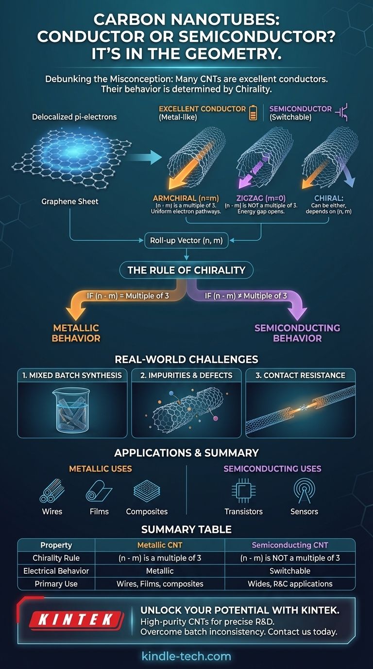
The core principle is this: a carbon nanotube is a rolled-up sheet of graphene. Its electrical conductivity is not an inherent property of the carbon itself, but is dictated by the precise angle at which that sheet is "rolled"—a geometric property known as chirality.
The Foundation: From Graphene to Nanotubes
To understand why a nanotube's geometry dictates its function, we must first look at its building block: graphene.
The Graphene Sheet
Graphene is a single, one-atom-thick layer of carbon atoms arranged in a honeycomb lattice. This unique structure is the source of its remarkable electronic properties.
Mobile "Pi-Electrons"
Each carbon atom in the lattice has one electron, a pi-electron, that is not locked into a bond between two atoms. Instead, these electrons are delocalized across the entire sheet, forming a sea of mobile charge carriers that can move freely, making graphene an exceptional conductor.
The "Roll-up" Vector
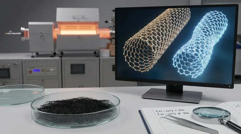
A carbon nanotube is formed when this 2D graphene sheet is conceptually rolled into a seamless 1D cylinder. The specific way it is rolled is defined by its chiral vector, represented by the indices (n, m).
How Geometry Determines Electrical Behavior
The simple act of rolling the 2D sheet into a 1D tube imposes strict rules on how electrons can travel, a phenomenon known as quantum confinement. This confinement is what separates one type of nanotube from another.
The Rule of Chirality
The relationship between the chiral indices (n, m) and the resulting electrical property is remarkably precise.
A simple mathematical rule emerges:
- If (n - m) is a multiple of 3, the nanotube will behave like a metal.
- If (n - m) is not a multiple of 3, the nanotube will behave like a semiconductor.
Why the Angle Matters
This rule exists because of how the electron's quantum wave functions interact with the nanotube's structure. In graphene, specific energy states allow for conduction.
When you roll the sheet, only certain electron pathways are allowed around the circumference of the tube. If the rolling angle (the chirality) allows these pathways to align with graphene's conductive states, the nanotube is metallic. If the angle causes them to miss these states, an energy gap (or band gap) opens up, and the nanotube is semiconducting.
Armchair vs. Zigzag and Chiral
The two most symmetric forms, "armchair" nanotubes (where n=m) and "zigzag" nanotubes (where m=0), illustrate this perfectly.
All armchair nanotubes are metallic because their (n-n)=0 structure always satisfies the "multiple of 3" rule. In contrast, zigzag and other chiral nanotubes can be either metallic or semiconducting, depending on their specific (n, m) values.
Common Pitfalls and Real-World Challenges
While the theory is clear, practical application faces significant hurdles that can lead to the perception of poor conductivity.
The Synthesis Problem
The single greatest challenge is that most production methods, like chemical vapor deposition, create a mixed batch of nanotubes. This resulting material is a random assortment of metallic and semiconducting types with various diameters and chiralities.
The Impact of Impurities
This mixture is often far less conductive than a pure sample of metallic CNTs would be. The semiconducting tubes act as barriers, and the junctions between different tubes create resistance, hindering overall electron flow.
Defects and Contact Resistance
Even a perfectly metallic nanotube can perform poorly if its atomic lattice has defects, which scatter electrons. Furthermore, making a clean, low-resistance electrical connection between a nanoscale tube and a macroscale wire is a persistent engineering problem.
Making the Right Choice for Your Goal
Understanding this principle is critical for applying carbon nanotubes in technology. Your objective determines which type of nanotube you need.
- If your primary focus is creating conductive composites, transparent films, or wires: Your goal is to maximize the percentage of metallic nanotubes in your material to create effective pathways for current.
- If your primary focus is building next-generation electronics like transistors: You require extremely pure semiconducting nanotubes, as their ability to have their conductivity switched "on" and "off" is the basis of digital logic.
Ultimately, the electrical nature of a carbon nanotube is a profound example of how a simple change in geometry at the nanoscale dictates its fundamental properties.
Summary Table:
| Property | Metallic CNT | Semiconducting CNT |
|---|---|---|
| Chirality Rule | (n - m) is a multiple of 3 | (n - m) is not a multiple of 3 |
| Electrical Behavior | Excellent conductor, like a metal | Conductivity can be switched on/off |
| Primary Use | Conductive composites, films, wires | Transistors, electronic devices |
Unlock the potential of carbon nanotubes in your lab.
The electrical properties of your carbon nanotube materials are critical to your project's success. Whether you need highly conductive metallic CNTs for advanced composites or pure semiconducting CNTs for next-generation electronics, the quality and specificity of your materials matter.
KINTEK specializes in providing high-purity lab equipment and consumables to meet your precise laboratory needs. Our expertise ensures you get the right materials for your research and development, helping you overcome challenges like batch inconsistency and impurities.
Let's discuss your application. Contact our experts today to find the perfect CNT solution for your work.
Visual Guide
Related Products
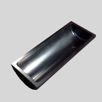
- Carbon Graphite Boat -Laboratory Tube Furnace with Cover
- Boron Nitride (BN) Ceramic Tube
- Hexagonal Boron Nitride HBN Thermocouple Protection Tube
People Also Ask
- What metals can you melt in a graphite crucible? A Guide to Safe & Efficient Melting
- Why is a graphite crucible containing molten bismuth used in LiF–NaF–KF purification? Enhance Melt Purity Efficiently
- Does a graphite crucible need to be seasoned? The Critical First-Use Safety Guide
- Why is graphite used in furnaces? For Extreme Heat, Purity, and Efficiency
- What is the use of graphite tube? Essential for Extreme Heat & Corrosive Environments
