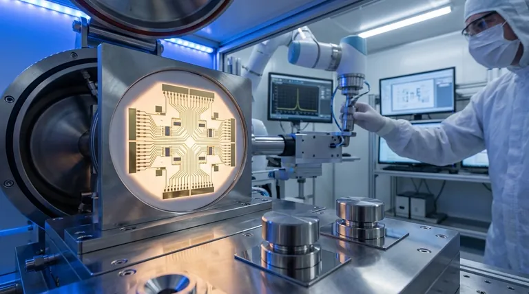
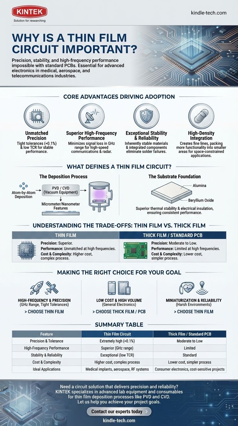
Thin film circuits are important because they provide a level of precision, stability, and high-frequency performance that is impossible to achieve with standard printed circuit boards or even thick film technology. Their manufacturing process, which involves depositing materials atom by atom in a vacuum, allows for the creation of extremely small and highly accurate components essential for advanced electronics in the medical, aerospace, and telecommunications industries.
While standard circuit fabrication is sufficient for most consumer electronics, it fails in applications demanding extreme precision and reliability. Thin film technology fills this critical gap, enabling the high-performance, miniaturized devices that power our most advanced systems.
What Defines a Thin Film Circuit?
The importance of thin film circuits stems directly from how they are made. Unlike a standard PCB where components are soldered on, or thick film where pastes are screen-printed, thin film circuits are built up layer by layer on a stable substrate.
The Deposition Process
The core of this technology is the deposition process, often physical vapor deposition (PVD) or chemical vapor deposition (CVD). These methods, which require sophisticated vacuum equipment, deposit extremely thin layers of conductive, resistive, or insulating material onto a substrate.
This meticulous process allows for circuit traces and components with features measured in micrometers or even nanometers, offering a degree of control that is orders of magnitude greater than other methods.
The Substrate Foundation
Thin film circuits are typically built on ceramic substrates like alumina or beryllium oxide. These materials offer superior thermal stability and electrical insulation compared to the FR-4 material used in standard PCBs.
This stable foundation ensures the circuit's performance remains consistent across a wide range of temperatures and operating conditions.
Core Advantages Driving Adoption
The unique manufacturing process gives thin film circuits four key advantages that make them indispensable for certain applications.
Unmatched Component Precision
Thin film deposition can create resistors and capacitors with extremely tight tolerances (often below 0.1%) and a very low Temperature Coefficient of Resistance (TCR). This means their electrical values change very little with temperature, ensuring stable performance.
Superior High-Frequency Performance
At RF and microwave frequencies (GHz range), the precise geometry and smooth surfaces of thin film conductors minimize signal loss and unpredictable electrical behavior (parasitics). This makes them essential for high-speed communications, radar, and satellite systems.
Exceptional Stability and Reliability
The materials used, such as tantalum nitride for resistors, are inherently stable and robust. The integrated nature of the circuit—where components are part of the substrate itself—eliminates solder joints, a common point of failure in conventional electronics.
High-Density Integration
The ability to create exceptionally fine lines and spaces allows engineers to pack more functionality into a much smaller physical area. This miniaturization is critical for implantable medical devices, compact sensor modules, and other space-constrained applications.
Understanding the Trade-offs: Thin Film vs. Thick Film
To truly understand why thin film is important, it's useful to compare it to its closest alternative, thick film technology.
Precision vs. Cost
Thin film provides superior precision at a higher cost. The vacuum deposition equipment and cleanroom environments required are expensive.
Thick film, which uses a simpler screen-printing process, is significantly cheaper and ideal for applications where cost is a primary driver and ultra-high precision is not needed.
Performance vs. Simplicity
The performance of thin film circuits at high frequencies is unmatched. However, the manufacturing process is complex.
Thick film fabrication is a much simpler, higher-throughput process, but it cannot achieve the fine features or performance characteristics required for demanding RF or optical applications.
Power Handling
In some cases, the thicker conductive layers of thick film circuits can allow them to handle higher currents than their thin film counterparts, though this is a generalized trade-off.
Making the Right Choice for Your Goal
Selecting the correct circuit fabrication method depends entirely on your project's technical and commercial requirements.
- If your primary focus is high-frequency performance and precision: Thin film is the only viable choice for applications in the GHz range or those requiring tight component tolerances.
- If your primary focus is low cost and high volume for general electronics: Standard PCBs or thick film technology offer a more economical and practical solution.
- If your primary focus is miniaturization and reliability in harsh environments: Thin film's stability and high-density capabilities make it the superior option for medical, aerospace, and military-grade hardware.
By understanding these fundamental differences, you can select the technology that provides the necessary performance without over-engineering your solution.
Summary Table:
| Feature | Thin Film Circuit | Thick Film / Standard PCB |
|---|---|---|
| Precision & Tolerance | Extremely high (<0.1%) | Moderate to Low |
| High-Frequency Performance | Superior (GHz range) | Limited |
| Stability & Reliability | Exceptional (low TCR) | Standard |
| Cost & Complexity | Higher cost, complex process | Lower cost, simpler process |
| Ideal Applications | Medical implants, aerospace, RF systems | Consumer electronics, cost-sensitive projects |
Need a circuit solution that delivers precision and reliability for demanding environments? KINTEK specializes in advanced lab equipment and consumables for thin film deposition processes like PVD and CVD. Our expertise supports the creation of high-performance circuits for the medical, aerospace, and telecommunications industries. Let us help you achieve your project goals with technology that meets the highest standards. Contact our experts today to discuss your specific needs!
Visual Guide
Related Products
- Electron Beam Evaporation Coating Oxygen-Free Copper Crucible and Evaporation Boat
- Thin-Layer Spectral Electrolysis Electrochemical Cell
People Also Ask
- What is the voltage of e-beam evaporation? Achieve Precise Thin-Film Deposition
- What is e-beam evaporation? Achieve High-Purity Thin Film Deposition for Your Lab
- How is an electron beam evaporator cooled during deposition? Essential Thermal Management for Stable Processes
- What are the applications of electron beams? From Nanoscale Imaging to Industrial Manufacturing
- What is the container that holds the metal source material called in e-beam evaporation? Ensure Purity and Quality in Your Thin-Film Deposition

