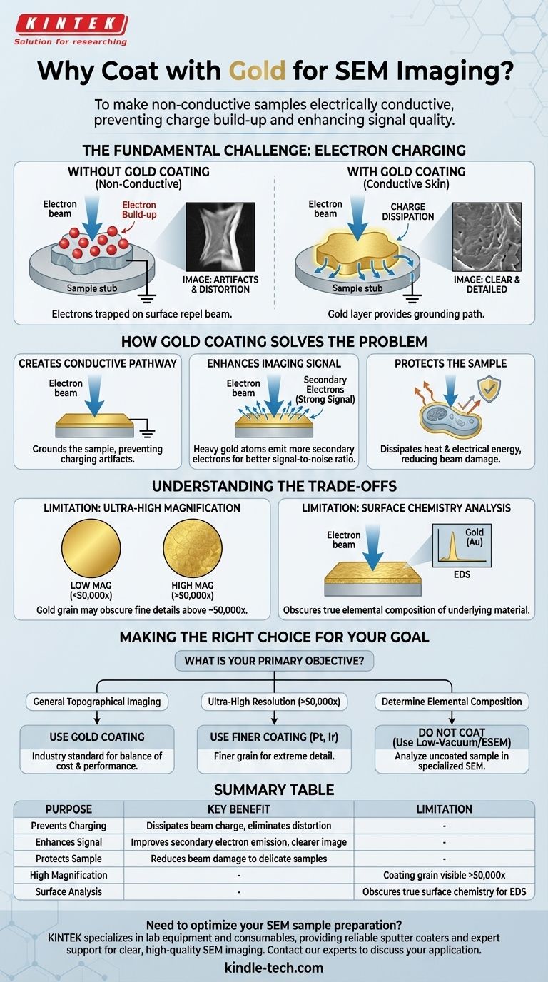
In short, an object is coated with gold before SEM imaging to make it electrically conductive. This thin gold layer prevents a destructive build-up of electron charge on the sample's surface, which would otherwise severely distort or completely ruin the image, and it also significantly enhances the signal quality for a clearer picture.
The core problem is that a Scanning Electron Microscope (SEM) uses an electron beam, and non-conductive materials like plastics or biological tissue can't dissipate the electrical charge from that beam. Gold coating creates a conductive "skin" that grounds the sample, solving this fundamental incompatibility and enabling clear imaging.
The Fundamental Challenge: Electrons and Insulators
To understand the role of gold, you must first understand the core problem it solves. An SEM doesn't work like a standard light microscope; it uses a focused beam of electrons to "see."
The Problem of "Charging"
SEM imaging works by scanning an electron beam across a sample. When these electrons hit the surface, they need a path to flow away to an electrical ground.
On a conductive material like metal, this happens automatically. On a non-conductive (insulating) material like a polymer, ceramic, or biological cell, the electrons have nowhere to go. They accumulate on the surface in a phenomenon known as charging.
The Consequences of Charging
This trapped electrical charge is disastrous for imaging. It creates a strong negative field that repels and deflects the incoming electron beam.
This deflection results in severe image artifacts, including bright, washed-out patches, distorted shapes, and a complete loss of fine detail. In extreme cases, the sample will simply appear as a bright white flare, making imaging impossible.
How Gold Coating Solves the Problem
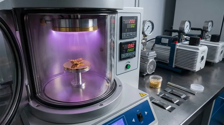
Applying a micro-thin layer of gold is the standard solution for non-conductive samples. This process, typically done via sputter coating, addresses the core issues in three distinct ways.
1. Creating a Conductive Pathway
The most critical function of the gold layer is to provide a path for electrical charge to dissipate. The gold "skin" is connected to the metal sample holder (the "stub"), which is grounded.
This allows the electrons from the microscope's beam to flow harmlessly off the sample surface, completely preventing the charging artifacts that would otherwise occur.
2. Enhancing the Imaging Signal
The image you see from an SEM is primarily constructed from secondary electrons—low-energy electrons that are knocked off the sample's surface by the primary beam.
Heavy metals like gold are exceptionally good at emitting secondary electrons. By coating the sample, you are essentially creating a surface that generates a much stronger, clearer signal for the SEM's detectors, dramatically improving the signal-to-noise ratio of the final image.
3. Protecting the Sample
The intense energy of an electron beam can damage delicate samples, especially biological tissue or plastics. This is known as beam damage.
The conductive gold layer helps to dissipate both heat and electrical energy across the surface, reducing localized damage and helping to preserve the sample's original structure during imaging.
Understanding the Trade-offs
While gold is an excellent general-purpose coating, it is not a perfect solution for every scenario. Understanding its limitations is key to good microscopy.
Gold is Not for Ultra-High Magnification
Gold has a relatively large grain size. At low to medium magnifications (typically under ~50,000x), this texture is too small to be seen and doesn't interfere with the image.
However, at very high magnifications, the granular structure of the gold coating itself can become visible, obscuring the finest details of your sample. For these applications, finer-grained (but more expensive) metals like platinum or iridium are preferred.
The Coating Obscures Surface Chemistry
An SEM can be equipped with detectors (like EDS) to determine the elemental composition of a sample. Because the electron beam interacts with the gold coating, any such analysis will simply detect gold, not the underlying material.
If your goal is to analyze the true surface chemistry of a non-conductive sample, you must avoid coating and instead use a specialized low-vacuum or environmental SEM (ESEM).
Making the Right Choice for Your Goal
The decision to use gold coating—or any coating at all—depends entirely on your imaging objective.
- If your primary focus is general topographical imaging of a non-conductive sample: Gold sputter coating is the industry standard, offering a fantastic balance of performance, cost, and ease of use.
- If your primary focus is ultra-high resolution imaging (well above 50,000x): You should use a finer-grained coating like platinum/palladium or iridium to ensure the coating's texture does not limit your resolution.
- If your primary focus is determining the elemental composition of the surface: Do not use a conductive coating. You must use an uncoated sample in a low-vacuum or variable-pressure SEM.
Ultimately, gold coating is a powerful preparatory technique that allows us to visualize the intricate, non-conductive world with the power of an electron beam.
Summary Table:
| Purpose of Gold Coating | Key Benefit |
|---|---|
| Prevents Charging | Dissipates electron beam charge to eliminate image distortion. |
| Enhances Signal | Improves secondary electron emission for a clearer image. |
| Protects Sample | Reduces beam damage to delicate samples like biological tissue. |
| Limitation: High Magnification | Coating grain may be visible above ~50,000x magnification. |
| Limitation: Surface Analysis | Obscures true surface chemistry for EDS analysis. |
Need to optimize your SEM sample preparation? KINTEK specializes in lab equipment and consumables, providing reliable sputter coaters and expert support to ensure your non-conductive samples are perfectly prepared for clear, high-quality SEM imaging. Contact our experts today to discuss your specific application and find the ideal solution for your laboratory needs.
Visual Guide
Related Products
- Electron Beam Evaporation Coating Gold Plating Tungsten Molybdenum Crucible for Evaporation
- Custom CVD Diamond Coating for Lab Applications
- HFCVD Machine System Equipment for Drawing Die Nano-Diamond Coating
- High Purity Gold Platinum Copper Iron Metal Sheets
People Also Ask
- What is the container that holds the metal source material called in e-beam evaporation? Ensure Purity and Quality in Your Thin-Film Deposition
- What materials are used in electron beam evaporation? Master High-Purity Thin Film Deposition
- What is the voltage of e-beam evaporation? Achieve Precise Thin-Film Deposition
- What is the temperature of e-beam evaporation? Mastering the Two-Zone Thermal Process for Precision Films
- What are the applications of e-beam evaporation? Achieve High-Purity Coatings for Optics & Electronics