Lab Materials
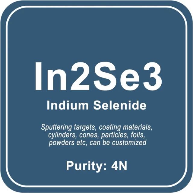
Indium Selenide (In2Se3) Sputtering Target / Powder / Wire / Block / Granule
Item Number : LM-In2Se3
Price varies based on specs and customizations
- Chemical Formula
- In2Se3
- Purity
- 4N
- Shape
- discs / wire / block / powder / plates / column targets / step target / custom-made

Shipping:
Contact us to get shipping details Enjoy On-time Dispatch Guarantee.
We offer Indium Selenide (In2Se3) materials at reasonable prices for your research needs. With our expertise, we can produce and tailor Indium Selenide (In2Se3) materials of different purities, shapes, and sizes to meet your specific requirements.
We offer a diverse range of specifications and sizes for sputtering targets (including circular, square, tubular, and irregular shapes), coating materials, cylinders, cones, particles, foils, powders, 3D printing powders, nanometer powders, wire rods, ingots, blocks, and more.
Details

About Indium Selenide (In2Se3)
Indium(III) Selenide is a semiconducting compound of the III-VI type that crystallizes in a lattice structure.
Indium(III) selenide is a compound of indium and selenium. It has potential for use in photovoltaic devices and it has been the subject of extensive research. The band-gap of γ-In2Se3 is approximately 1.9 eV.
The two most common phases, α and β, have a layered structure, while γ is a "defect wurtzite structure." In all, there are five known forms (α, β, γ, δ, κ). The α- β phase transition is accompanied by a change in electrical conductivity.
The crystalline form of a sample can depend on the method of production. For example, thin films of pure γ-In2Se3 have been produced from trimethylindium, InMe3, and hydrogen selenide, H2Se, using MOCVD techniques. A synthetic procedure to encapsulate single layer β-In2Se3 nanoribbons inside carbon nanotubes has been developed.
The encapsulated nanoribbons undergo a thermally induced phase change to γ-In2Se3 nanowires following heating to 400 °C.
Ingredient Quality Control
- Raw material composition analysis
- Through the use of equipment such as ICP and GDMS, the content of metal impurities is detected and analyzed to ensure that it meets the purity standard;
Non-metallic impurities are detected by equipment such as carbon and sulfur analyzers, nitrogen and oxygen analyzers. - Metallographic flaw detection analysis
- The target material is inspected using flaw detection equipment to ensure that there are no defects or shrinkage holes inside the product;
Through metallographic testing, the internal grain structure of the target material is analyzed to ensure that the grains are fine and dense. - Appearance and dimension inspection
- Product dimensions are measured using micrometers and precision calipers to ensure compliance with drawings;
The surface finish and cleanliness of the product are measured using a surface cleanliness meter.
Conventional Sputtering Target Sizes
- Preparation process
- hot isostatic pressing, vacuum melting, etc.
- Sputtering target shape
- plane sputtering target, multi-arc sputtering target, step sputtering target, special-shaped sputtering target
- Round sputtering target size
- Diameter: 25.4mm / 50mm / 50.8mm / 60mm / 76.2mm / 80mm / 100mm / 101.6mm / 152.4mm
Thickness: 3mm / 4mm / 5mm / 6mm / 6.35mm
Size can be customized. - Square sputtering target size
- 50×50×3mm / 100×100×4mm / 300×300×5mm, size can be customized
Available Metal Forms
Metal Forms Details
We manufacture almost all the metals listed on the periodic table in a wide range of forms and purities, as well as standard sizes and dimensions. We can also produce custom-made products to meet specific customer requirements, such as size, shape, surface area, composition, and more. The following list provides a sample of the forms we offer, but it is not exhaustive. If you need laboratory consumables, please contact us directly to request a quote.
- Flat/Planar Forms: Board, Film, Foil, Microfoil, Microleaf, Paper, Plate, Ribbon, Sheet, Strip, Tape, Wafer
- Preformed Shapes: Anodes, Balls, Bands, Bars, Boats, Bolts, Briquettes, Cathodes, Circles, Coils, Crucibles, Crystals, Cubes, Cups, Cylinders, Discs, Electrodes, Fibers, Filaments, Flanges, Grids, Lenses, Mandrels, Nuts, Parts, Prisms, Pucks, Rings, Rods, Shapes, Shields, Sleeves, Springs, Squares, Sputtering Targets, Sticks, Tubes, Washers, Windows, Wires
- Microsizes: Beads, Bits, Capsules, Chips, Coins, Dust, Flakes, Grains, Granules, Micropowder, Needles, Particles, Pebbles, Pellets, Pins, Pills, Powder, Shavings, Shot, Slugs, Spheres, Tablets
- Macrosizes: Billets, Chunks, Cuttings, Fragments, Ingots, Lumps, Nuggets, Pieces, Punchings, Rocks, Scraps, Segments, Turnings
- Porous and Semi-Porous: Fabric, Foam, Gauze, Honeycomb, Mesh, Sponge, Wool
- Nanoscale: Nanoparticles, Nanopowders, Nanofoils, Nanotubes, Nanorods, Nanoprisms
- Others: Concentrate, Ink, Paste, Precipitate, Residue, Samples, Specimens
KinTek specializes in the manufacturing of high-purity and ultra-high-purity materials with a purity range of 99.999% (5N), 99.9999% (6N), 99.99995% (6N5), and in some cases, up to 99.99999% (7N). Our materials are available in specific grades, including UP/UHP, semiconductor, electronic, deposition, fiber optic, and MBE grades. Our high-purity metals, oxides, and compounds are specifically crafted to meet the rigorous demands of high-technology applications and are ideal for use as dopants and precursor materials for thin film deposition, crystal growth of semiconductors, and synthesis of nanomaterials. These materials find use in advanced microelectronics, solar cells, fuel cells, optical materials, and other cutting-edge applications.
Packaging
We use vacuum packaging for our high-purity materials, and each material has specific packaging tailored to its unique characteristics. For instance, our Hf sputter target is externally tagged and labeled to facilitate efficient identification and quality control. We take great care to prevent any damage that could occur during storage or transportation.
4.8
out of
5
Their Indium Selenide (In2Se3) is really worth the money. It's worth every penny.
4.9
out of
5
I highly recommend KINTEK SOLUTION's products. Their commitment to quality and customer satisfaction is evident in the superior quality of their materials.
4.7
out of
5
The delivery was quicker than I expected, and the quality of the product is exceptional. Very satisfied with my purchase.
4.8
out of
5
The technological advancement of their products is truly impressive. They continuously innovate to meet the evolving needs of the industry.
4.6
out of
5
KINTEK SOLUTION's Indium Selenide (In2Se3) is a game-changer for our research. Its durability and reliability have been exceptional.
4.9
out of
5
The quality of their Indium Selenide (In2Se3) is outstanding. The consistency in performance is commendable.
4.7
out of
5
The customer service at KINTEK SOLUTION is top-notch. They go above and beyond to ensure customer satisfaction.
4.8
out of
5
KINTEK SOLUTION's commitment to quality and innovation is reflected in the exceptional products they offer. Highly satisfied with my experience.
REQUEST A QUOTE
Our professional team will reply to you within one business day. Please feel free to contact us!
Related Products
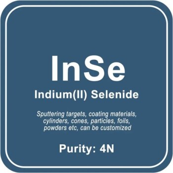
Indium(II) Selenide (InSe) Sputtering Target / Powder / Wire / Block / Granule
Looking for high-quality Indium(II) Selenide materials for your lab at reasonable prices? Our tailored and customizable InSe products come in various purities, shapes, and sizes to suit your unique needs. Choose from a range of sputtering targets, coating materials, powders, and more.
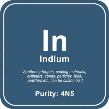
High Purity Indium (In) Sputtering Target / Powder / Wire / Block / Granule
Looking for high-quality Indium materials for laboratory use? Look no further! Our expertise lies in producing tailored Indium materials of varying purities, shapes, and sizes. We offer a wide range of Indium products to suit your unique requirements. Order now at reasonable prices!
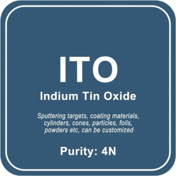
High Purity Indium Tin Oxide (ITO) Sputtering Target / Powder / Wire / Block / Granule
Get high-quality Indium Tin Oxide (ITO) Sputtering Targets for your lab needs at reasonable prices. Our customized options of different shapes and sizes cater to your unique requirements. Browse our range today.
Zinc Selenide (ZnSe) Sputtering Target / Powder / Wire / Block / Granule
Looking for Zinc Selenide (ZnSe) materials for your laboratory? Our affordable prices and expertly tailored options make us the perfect choice. Explore our wide range of specifications and sizes today!
High Purity Selenium (Se) Sputtering Target / Powder / Wire / Block / Granule
Looking for affordable Selenium (Se) materials for laboratory use? We specialize in producing and tailoring materials of various purities, shapes, and sizes to suit your unique requirements. Explore our range of sputtering targets, coating materials, powders, and more.

Copper Nickel Indium Alloy (CuNiIn) Sputtering Target / Powder / Wire / Block / Granule
Looking for Copper Nickel Indium materials for your lab? Our affordable products come in different purities, shapes, and sizes to fit your needs. Browse our sputtering targets, powders, foils, and more!
Zinc Sulfide (ZnS) Sputtering Target / Powder / Wire / Block / Granule
Get affordable Zinc Sulfide (ZnS) materials for your laboratory needs. We produce and customize ZnS materials of varying purities, shapes, and sizes. Choose from a wide range of sputtering targets, coating materials, powders, and more.

Tungsten Sulfide (WS2) Sputtering Target / Powder / Wire / Block / Granule
Looking for Tungsten Sulfide (WS2) materials for your lab? We offer a range of customizable options at great prices, including sputtering targets, coating materials, powders, and more. Order now!
Infrared Silicon / High Resistance Silicon / Single Crystal Silicon Lens
Silicon (Si) is widely regarded as one of the most durable mineral and optical materials for applications in the near-infrared (NIR) range, approximately 1 μm to 6 μm.
Tin Sulfide (SnS2) Sputtering Target / Powder / Wire / Block / Granule
Find high-quality Tin Sulfide (SnS2) materials for your laboratory at affordable prices. Our experts produce and customize materials to meet your specific needs. Check out our range of sputtering targets, coating materials, powders, and more.
High Purity Silicon Dioxide (SiO2) Sputtering Target / Powder / Wire / Block / Granule
Looking for Silicon Dioxide materials for your lab? Our expertly tailored SiO2 materials come in various purities, shapes, and sizes. Browse our wide range of specifications today!
Optics Zinc Sulphide (ZnS) Windows have an excellent IR transmission range between 8-14 microns.Excellent mechanical strength and chemical inertness for harsh environments (harder than ZnSe Windows)
Molybdenum Carbide (Mo2C) Sputtering Target / Powder / Wire / Block / Granule
Looking for high-quality Molybdenum Carbide (Mo2C) materials for your lab? Look no further! Our expertly-produced materials come in a range of purities, shapes, and sizes to meet your unique needs. Shop sputtering targets, coatings, powders, and more today.
Antimony Sulfide (Sb2S3) Sputtering Target / Powder / Wire / Block / Granule
Get high-quality Antimony Sulfide (Sb2S3) materials for your laboratory at reasonable prices. Our customizable products include sputtering targets, powders, foils, and more. Order now!
Infrared thermal imaging / infrared temperature measurement double-sided coated germanium (Ge) lens
Germanium lenses are durable, corrosion-resistant optical lenses suited for harsh environments and applications exposed to the elements.
Molybdenum Sulfide (MoS2) Sputtering Target / Powder / Wire / Block / Granule
Find high-quality Molybdenum Sulfide materials at reasonable prices for your laboratory needs. Customized shapes, sizes, and purities available. Browse our selection of sputtering targets, powders, and more.
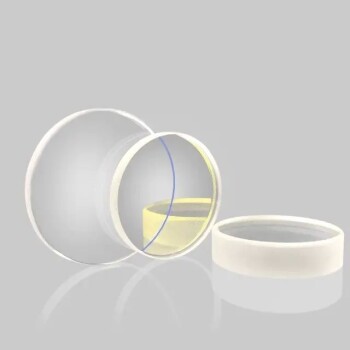
Zinc selenide(ZnSe) window / substrate / optical lens
Zinc selenide is formed by synthesizing zinc vapor with H2Se gas, resulting in sheet-like deposits on graphite susceptors.
Cobalt Silicide (CoSi2) Sputtering Target / Powder / Wire / Block / Granule
Looking for affordable Cobalt Silicide materials for your laboratory research? We offer tailored solutions of different purities, shapes, and sizes, including sputtering targets, coating materials, and more. Explore our range now!
Silicon Carbide (SiC) Sputtering Target / Powder / Wire / Block / Granule
Looking for high-quality Silicon Carbide (SiC) materials for your lab? Look no further! Our expert team produces and tailors SiC materials to your exact needs at reasonable prices. Browse our range of sputtering targets, coatings, powders, and more today.

Silicon Carbide (SIC) Ceramic Sheet Flat / Corrugated Heat Sink
Silicon carbide (sic) ceramic heat sink not only does not generate electromagnetic waves, but also can isolate electromagnetic waves and absorb part of electromagnetic waves.
High Purity Germanium (Ge) Sputtering Target / Powder / Wire / Block / Granule
Get high-quality gold materials for your laboratory needs at affordable prices. Our custom-made gold materials come in various shapes, sizes, and purities to fit your unique requirements. Explore our range of sputtering targets, coating materials, foils, powders, and more.
Cobalt Telluride (CoTe) Sputtering Target / Powder / Wire / Block / Granule
Get high-quality Cobalt Telluride materials for your laboratory needs at reasonable prices. We offer customized shapes, sizes, and purities, including sputtering targets, coatings, powders, and more.