Lab Materials
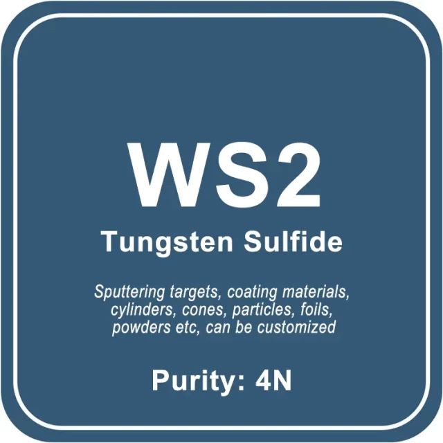
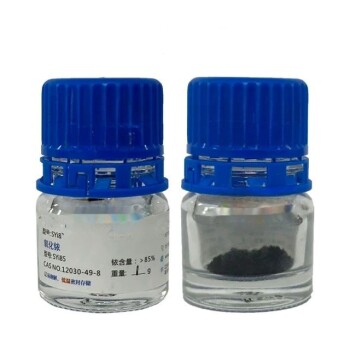
Tungsten Sulfide (WS2) Sputtering Target / Powder / Wire / Block / Granule
Item Number : LM-WS2
Price varies based on specs and customizations
- Chemical Formula
- WS2
- Purity
- 4N
- Shape
- discs / wire / block / powder / plates / column targets / step target / custom-made

Shipping:
Contact us to get shipping details Enjoy On-time Dispatch Guarantee.
At affordable prices, we offer Tungsten Sulfide (WS2) materials for laboratory use. Our proficiency lies in producing and customizing Tungsten Sulfide (WS2) materials with varying purities, shapes, and sizes to cater to your specific needs.
Our selection of sputtering targets (circular, square, tubular, irregular), coating materials, cylinders, cones, particles, foils, powders, 3D printing powders, nanometer powders, wire rods, ingots, and blocks are available in a variety of specifications and sizes.
Details


About Tungsten Sulfide (WS2)
Tungsten Sulfide is a soluble Tungsten source, compatible with sulfates. Sulfate compounds are formed by replacing one or both hydrogens with a metal, and are usually readily soluble in water for water treatment purposes. On the other hand, fluorides and oxides are typically insoluble.
Organometallic forms of Tungsten Sulfide are soluble in both organic and aqueous solutions. Additionally, metallic ions can be dispersed using suspended or coated nanoparticles and deposited using sputtering targets and evaporation materials. These applications are common in fields such as solar energy materials and fuel cells.
Tungsten Sulfide is generally available in most volumes, and its ultra high purity and high purity compositions can enhance its optical quality and use as a scientific standard. Alternatively, nanoscale elemental powders and suspensions can be utilized to form high surface area structures.
Ingredient Quality Control
- Raw material composition analysis
- Through the use of equipment such as ICP and GDMS, the content of metal impurities is detected and analyzed to ensure that it meets the purity standard;
Non-metallic impurities are detected by equipment such as carbon and sulfur analyzers, nitrogen and oxygen analyzers. - Metallographic flaw detection analysis
- The target material is inspected using flaw detection equipment to ensure that there are no defects or shrinkage holes inside the product;
Through metallographic testing, the internal grain structure of the target material is analyzed to ensure that the grains are fine and dense. - Appearance and dimension inspection
- Product dimensions are measured using micrometers and precision calipers to ensure compliance with drawings;
The surface finish and cleanliness of the product are measured using a surface cleanliness meter.
Conventional Sputtering Target Sizes
- Preparation process
- hot isostatic pressing, vacuum melting, etc.
- Sputtering target shape
- plane sputtering target, multi-arc sputtering target, step sputtering target, special-shaped sputtering target
- Round sputtering target size
- Diameter: 25.4mm / 50mm / 50.8mm / 60mm / 76.2mm / 80mm / 100mm / 101.6mm / 152.4mm
Thickness: 3mm / 4mm / 5mm / 6mm / 6.35mm
Size can be customized. - Square sputtering target size
- 50×50×3mm / 100×100×4mm / 300×300×5mm, size can be customized
Available Metal Forms
Metal Forms Details
We manufacture almost all the metals listed on the periodic table in a wide range of forms and purities, as well as standard sizes and dimensions. We can also produce custom-made products to meet specific customer requirements, such as size, shape, surface area, composition, and more. The following list provides a sample of the forms we offer, but it is not exhaustive. If you need laboratory consumables, please contact us directly to request a quote.
- Flat/Planar Forms: Board, Film, Foil, Microfoil, Microleaf, Paper, Plate, Ribbon, Sheet, Strip, Tape, Wafer
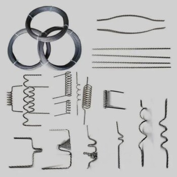
- Preformed Shapes: Anodes, Balls, Bands, Bars, Boats, Bolts, Briquettes, Cathodes, Circles, Coils, Crucibles, Crystals, Cubes, Cups, Cylinders, Discs, Electrodes, Fibers, Filaments, Flanges, Grids, Lenses, Mandrels, Nuts, Parts, Prisms, Pucks, Rings, Rods, Shapes, Shields, Sleeves, Springs, Squares, Sputtering Targets, Sticks, Tubes, Washers, Windows, Wires
- Microsizes: Beads, Bits, Capsules, Chips, Coins, Dust, Flakes, Grains, Granules, Micropowder, Needles, Particles, Pebbles, Pellets, Pins, Pills, Powder, Shavings, Shot, Slugs, Spheres, Tablets
- Macrosizes: Billets, Chunks, Cuttings, Fragments, Ingots, Lumps, Nuggets, Pieces, Punchings, Rocks, Scraps, Segments, Turnings
- Porous and Semi-Porous: Fabric, Foam, Gauze, Honeycomb, Mesh, Sponge, Wool
- Nanoscale: Nanoparticles, Nanopowders, Nanofoils, Nanotubes, Nanorods, Nanoprisms
- Others: Concentrate, Ink, Paste, Precipitate, Residue, Samples, Specimens
KinTek specializes in the manufacturing of high-purity and ultra-high-purity materials with a purity range of 99.999% (5N), 99.9999% (6N), 99.99995% (6N5), and in some cases, up to 99.99999% (7N). Our materials are available in specific grades, including UP/UHP, semiconductor, electronic, deposition, fiber optic, and MBE grades. Our high-purity metals, oxides, and compounds are specifically crafted to meet the rigorous demands of high-technology applications and are ideal for use as dopants and precursor materials for thin film deposition, crystal growth of semiconductors, and synthesis of nanomaterials. These materials find use in advanced microelectronics, solar cells, fuel cells, optical materials, and other cutting-edge applications.
Packaging
We use vacuum packaging for our high-purity materials, and each material has specific packaging tailored to its unique characteristics. For instance, our Hf sputter target is externally tagged and labeled to facilitate efficient identification and quality control. We take great care to prevent any damage that could occur during storage or transportation.
4.7
out of
5
The prompt delivery and outstanding quality of the Tungsten Sulfide (WS2) materials from KINTEK SOLUTION are truly remarkable.
4.8
out of
5
KINTEK SOLUTION's Tungsten Sulfide (WS2) materials are an exceptional value for money. Their durability and performance are top-notch.
4.9
out of
5
KINTEK SOLUTION's Tungsten Sulfide (WS2) materials have consistently exceeded our expectations in terms of quality and consistency.
4.7
out of
5
The technological advancements incorporated into KINTEK SOLUTION's Tungsten Sulfide (WS2) materials are truly impressive, enabling us to push the boundaries of our research.
4.8
out of
5
KINTEK SOLUTION's Tungsten Sulfide (WS2) materials have proven to be an invaluable asset in our laboratory, providing reliable and accurate results time and again.
4.9
out of
5
The exceptional quality and consistency of KINTEK SOLUTION's Tungsten Sulfide (WS2) materials have significantly enhanced the efficiency and productivity of our research.
4.7
out of
5
KINTEK SOLUTION's Tungsten Sulfide (WS2) materials have enabled us to achieve remarkable breakthroughs in our research, thanks to their superior performance and durability.
4.8
out of
5
The value for money offered by KINTEK SOLUTION's Tungsten Sulfide (WS2) materials is truly exceptional, making them an indispensable part of our laboratory budget.
4.9
out of
5
KINTEK SOLUTION's Tungsten Sulfide (WS2) materials have revolutionized our research, empowering us to explore new avenues and achieve groundbreaking results.
4.7
out of
5
The speed of delivery for KINTEK SOLUTION's Tungsten Sulfide (WS2) materials is truly remarkable, ensuring that our research projects stay on track and deadlines are met.
4.8
out of
5
KINTEK SOLUTION's Tungsten Sulfide (WS2) materials have consistently exceeded our expectations, providing exceptional quality and reliability that have transformed our research.
4.9
out of
5
The technological advancements embodied in KINTEK SOLUTION's Tungsten Sulfide (WS2) materials have enabled us to push the boundaries of scientific exploration and make groundbreaking discoveries.
4.7
out of
5
KINTEK SOLUTION's Tungsten Sulfide (WS2) materials have proven to be an invaluable asset, enabling us to conduct cutting-edge research and achieve remarkable results.
4.8
out of
5
The exceptional value for money offered by KINTEK SOLUTION's Tungsten Sulfide (WS2) materials makes them an indispensable choice for laboratories operating on tight budgets.
4.9
out of
5
KINTEK SOLUTION's Tungsten Sulfide (WS2) materials have revolutionized our research, enabling us to achieve unprecedented levels of accuracy and precision in our experiments.
4.7
out of
5
The speed of delivery for KINTEK SOLUTION's Tungsten Sulfide (WS2) materials is truly impressive, ensuring that our research projects proceed smoothly and efficiently.
4.8
out of
5
KINTEK SOLUTION's Tungsten Sulfide (WS2) materials have consistently exceeded our expectations, providing exceptional quality and reliability that have transformed our research.
4.9
out of
5
The technological advancements embodied in KINTEK SOLUTION's Tungsten Sulfide (WS2) materials have enabled us to push the boundaries of scientific exploration and make groundbreaking discoveries.
4.7
out of
5
KINTEK SOLUTION's Tungsten Sulfide (WS2) materials have proven to be an invaluable asset, enabling us to conduct cutting-edge research and achieve remarkable results.
REQUEST A QUOTE
Our professional team will reply to you within one business day. Please feel free to contact us!
Related Products
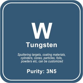
High Purity Tungsten (W) Sputtering Target / Powder / Wire / Block / Granule
Find high-quality Tungsten (W) materials for your laboratory needs at affordable prices. We offer customized purities, shapes, and sizes of sputtering targets, coating materials, powders, and more.
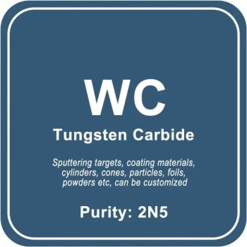
Tungsten Carbide (WC) Sputtering Target / Powder / Wire / Block / Granule
Looking for affordable Tungsten Carbide (WC) materials for your lab? Our expertly tailored products come in various shapes and sizes, from sputtering targets to nanometer powders. Shop now for quality materials that fit your unique needs.
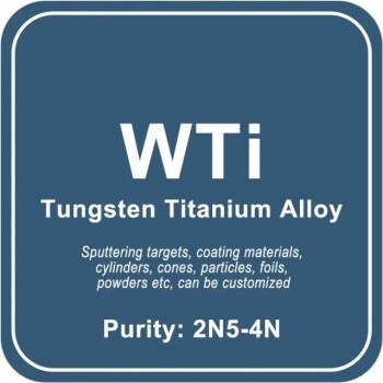
Tungsten Titanium Alloy (WTi) Sputtering Target / Powder / Wire / Block / Granule
Discover our Tungsten Titanium Alloy (WTi) materials for laboratory use at affordable prices. Our expertise allows us to produce custom materials of different purities, shapes, and sizes. Choose from a wide range of sputtering targets, powders, and more.
High Purity Tungsten Oxide (WO3) Sputtering Target / Powder / Wire / Block / Granule
Looking for high-quality Tungsten Oxide (WO3) materials? Our laboratory-grade products are tailored to your specific needs, with a range of purities, shapes, and sizes available. Shop sputtering targets, coating materials, and more.
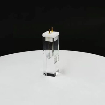
Thin-layer spectral electrolysis cell
Discover the benefits of our thin-layer spectral electrolysis cell. Corrosion-resistant, complete specifications, and customizable for your needs.
Zinc Sulfide (ZnS) Sputtering Target / Powder / Wire / Block / Granule
Get affordable Zinc Sulfide (ZnS) materials for your laboratory needs. We produce and customize ZnS materials of varying purities, shapes, and sizes. Choose from a wide range of sputtering targets, coating materials, powders, and more.
Molybdenum Sulfide (MoS2) Sputtering Target / Powder / Wire / Block / Granule
Find high-quality Molybdenum Sulfide materials at reasonable prices for your laboratory needs. Customized shapes, sizes, and purities available. Browse our selection of sputtering targets, powders, and more.
PTFE conductive glass substrate cleaning rack
The PTFE conductive glass substrate cleaning rack is used as the carrier of the square solar cell silicon wafer to ensure efficient and pollution-free handling during the cleaning process.
Tin Sulfide (SnS2) Sputtering Target / Powder / Wire / Block / Granule
Find high-quality Tin Sulfide (SnS2) materials for your laboratory at affordable prices. Our experts produce and customize materials to meet your specific needs. Check out our range of sputtering targets, coating materials, powders, and more.
Antimony Sulfide (Sb2S3) Sputtering Target / Powder / Wire / Block / Granule
Get high-quality Antimony Sulfide (Sb2S3) materials for your laboratory at reasonable prices. Our customizable products include sputtering targets, powders, foils, and more. Order now!
High Purity Silicon Dioxide (SiO2) Sputtering Target / Powder / Wire / Block / Granule
Looking for Silicon Dioxide materials for your lab? Our expertly tailored SiO2 materials come in various purities, shapes, and sizes. Browse our wide range of specifications today!
Thin proton exchange membrane with low resistivity; high proton conductivity; low hydrogen permeation current density; long life; suitable for electrolyte separators in hydrogen fuel cells and electrochemical sensors.
High Purity Silicon (Si) Sputtering Target / Powder / Wire / Block / Granule
Looking for high-quality Silicon (Si) materials for your laboratory? Look no further! Our custom-produced Silicon (Si) materials come in various purities, shapes, and sizes to suit your unique requirements. Browse our selection of sputtering targets, powders, foils, and more. Order now!
Tantalum Tungsten Alloy (TaW) Sputtering Target / Powder / Wire / Block / Granule
Looking for high-quality Tantalum Tungsten Alloy (TaW) materials? We offer a wide range of customizable options at competitive prices for laboratory use, including sputtering targets, coatings, powders, and more.
Thermally evaporated tungsten wire
It has a high melting point, thermal and electrical conductivity, and corrosion resistance. It is a valuable material for high temperature, vacuum and other industries.

Titanium Silicon Alloy (TiSi) Sputtering Target / Powder / Wire / Block / Granule
Discover our affordable Titanium Silicon Alloy (TiSi) materials for laboratory use. Our custom production offers various purities, shapes, and sizes for sputtering targets, coatings, powders, and more. Find the perfect match for your unique needs.

High Purity Tellurium (Te) Sputtering Target / Powder / Wire / Block / Granule
Discover our range of high-quality Tellurium (Te) materials for laboratory use at affordable prices. Our expert team produces custom sizes and purities to fit your unique needs. Shop sputtering targets, powders, ingots, and more.
Anion exchange membranes (AEMs) are semipermeable membranes, usually made of ionomers, designed to conduct anions but reject gases such as oxygen or hydrogen.

CVD Diamond Coating: Superior Thermal Conductivity, Crystal Quality, and Adhesion for Cutting Tools, Friction, and Acoustic Applications
TGPH060 Hydrophilic carbon paper
Toray carbon paper is a porous C/C composite material product (composite material of carbon fiber and carbon) that has undergone high-temperature heat treatment.

Elevate your experiments with our Platinum Sheet Electrode. Crafted with quality materials, our safe and durable models can be tailored to fit your needs.
Iridium dioxide IrO2 for electrolysis of water
Iridium dioxide, whose crystal lattice is rutile structure. Iridium dioxide and other rare metal oxides can be used in anode electrodes for industrial electrolysis and microelectrodes for electrophysiological research.
High Purity Carbon (C) Sputtering Target / Powder / Wire / Block / Granule
Looking for affordable Carbon (C) materials for your laboratory needs? Look no further! Our expertly produced and tailored materials come in a variety of shapes, sizes, and purities. Choose from sputtering targets, coating materials, powders, and more.
