Lab Materials
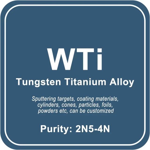
Tungsten Titanium Alloy (WTi) Sputtering Target / Powder / Wire / Block / Granule
Item Number : LM-WTi
Price varies based on specs and customizations
- Chemical Formula
- WTi
- Purity
- 2N5-4N
- Commonly Used Ratio
- W:Ti=90:10 wt%
- Shape
- discs / wire / block / powder / plates / column targets / step target / custom-made

Shipping:
Contact us to get shipping details Enjoy On-time Dispatch Guarantee.
Ingredient Quality Control
- Raw material composition analysis
- Through the use of equipment such as ICP and GDMS, the content of metal impurities is detected and analyzed to ensure that it meets the purity standard;
Non-metallic impurities are detected by equipment such as carbon and sulfur analyzers, nitrogen and oxygen analyzers. - Metallographic flaw detection analysis
- The target material is inspected using flaw detection equipment to ensure that there are no defects or shrinkage holes inside the product;
Through metallographic testing, the internal grain structure of the target material is analyzed to ensure that the grains are fine and dense. - Appearance and dimension inspection
- Product dimensions are measured using micrometers and precision calipers to ensure compliance with drawings;
The surface finish and cleanliness of the product are measured using a surface cleanliness meter.
Conventional Sputtering Target Sizes
- Preparation process
- hot isostatic pressing, vacuum melting, etc.
- Sputtering target shape
- plane sputtering target, multi-arc sputtering target, step sputtering target, special-shaped sputtering target
- Round sputtering target size
- Diameter: 25.4mm / 50mm / 50.8mm / 60mm / 76.2mm / 80mm / 100mm / 101.6mm / 152.4mm
Thickness: 3mm / 4mm / 5mm / 6mm / 6.35mm
Size can be customized. - Square sputtering target size
- 50×50×3mm / 100×100×4mm / 300×300×5mm, size can be customized
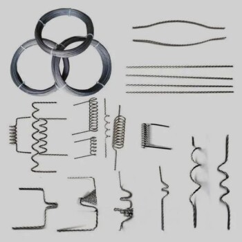
Available Metal Forms
Metal Forms Details
We manufacture almost all the metals listed on the periodic table in a wide range of forms and purities, as well as standard sizes and dimensions. We can also produce custom-made products to meet specific customer requirements, such as size, shape, surface area, composition, and more. The following list provides a sample of the forms we offer, but it is not exhaustive. If you need laboratory consumables, please contact us directly to request a quote.
- Flat/Planar Forms: Board, Film, Foil, Microfoil, Microleaf, Paper, Plate, Ribbon, Sheet, Strip, Tape, Wafer
- Preformed Shapes: Anodes, Balls, Bands, Bars, Boats, Bolts, Briquettes, Cathodes, Circles, Coils, Crucibles, Crystals, Cubes, Cups, Cylinders, Discs, Electrodes, Fibers, Filaments, Flanges, Grids, Lenses, Mandrels, Nuts, Parts, Prisms, Pucks, Rings, Rods, Shapes, Shields, Sleeves, Springs, Squares, Sputtering Targets, Sticks, Tubes, Washers, Windows, Wires
- Microsizes: Beads, Bits, Capsules, Chips, Coins, Dust, Flakes, Grains, Granules, Micropowder, Needles, Particles, Pebbles, Pellets, Pins, Pills, Powder, Shavings, Shot, Slugs, Spheres, Tablets
- Macrosizes: Billets, Chunks, Cuttings, Fragments, Ingots, Lumps, Nuggets, Pieces, Punchings, Rocks, Scraps, Segments, Turnings
- Porous and Semi-Porous: Fabric, Foam, Gauze, Honeycomb, Mesh, Sponge, Wool
- Nanoscale: Nanoparticles, Nanopowders, Nanofoils, Nanotubes, Nanorods, Nanoprisms
- Others: Concentrate, Ink, Paste, Precipitate, Residue, Samples, Specimens
KinTek specializes in the manufacturing of high-purity and ultra-high-purity materials with a purity range of 99.999% (5N), 99.9999% (6N), 99.99995% (6N5), and in some cases, up to 99.99999% (7N). Our materials are available in specific grades, including UP/UHP, semiconductor, electronic, deposition, fiber optic, and MBE grades. Our high-purity metals, oxides, and compounds are specifically crafted to meet the rigorous demands of high-technology applications and are ideal for use as dopants and precursor materials for thin film deposition, crystal growth of semiconductors, and synthesis of nanomaterials. These materials find use in advanced microelectronics, solar cells, fuel cells, optical materials, and other cutting-edge applications.
Packaging
We use vacuum packaging for our high-purity materials, and each material has specific packaging tailored to its unique characteristics. For instance, our Hf sputter target is externally tagged and labeled to facilitate efficient identification and quality control. We take great care to prevent any damage that could occur during storage or transportation.
FAQ
What Is Sputtering Target?
How Are Sputtering Targets Made?
What Is Sputtering Target Used For?
What Are Sputtering Targets For Electronics?
What Is The Lifetime Of A Sputtering Target?
4.8
out of
5
The Tungsten Titanium Alloy from KINTEK SOLUTION is an absolute game-changer! Their attention to detail and commitment to quality are evident in every product.
4.9
out of
5
KINTEK SOLUTION's Tungsten Titanium Alloy has been a lifesaver for our research. Its durability and reliability have enabled us to conduct experiments with confidence.
4.7
out of
5
The purity and consistency of KINTEK SOLUTION's Tungsten Titanium Alloy are top-notch. Highly recommended for any lab seeking high-quality materials.
4.6
out of
5
KINTEK SOLUTION's Tungsten Titanium Alloy is a testament to their expertise in materials science. Its performance has exceeded our expectations.
4.8
out of
5
The versatility of KINTEK SOLUTION's Tungsten Titanium Alloy is remarkable. It has proven invaluable in various applications within our lab.
4.9
out of
5
KINTEK SOLUTION's Tungsten Titanium Alloy is a game-changer for our research. Its exceptional properties have allowed us to break new ground in our field.
4.7
out of
5
The quality of KINTEK SOLUTION's Tungsten Titanium Alloy is unmatched. It has consistently met our stringent requirements, ensuring reliable results.
4.6
out of
5
KINTEK SOLUTION's Tungsten Titanium Alloy is worth every penny. Its durability and longevity have saved us both time and money in the long run.
4.8
out of
5
The customer service at KINTEK SOLUTION is outstanding. They go above and beyond to ensure that we receive our Tungsten Titanium Alloy orders promptly and efficiently.
4.9
out of
5
KINTEK SOLUTION's Tungsten Titanium Alloy is a marvel of materials science. Its unique properties have opened up new possibilities for our research.
4.7
out of
5
The purity of KINTEK SOLUTION's Tungsten Titanium Alloy is exceptional. It has enabled us to achieve unprecedented results in our experiments.
4.6
out of
5
KINTEK SOLUTION's Tungsten Titanium Alloy is a valuable asset to our lab. Its versatility and reliability have made it an indispensable tool for our research.
4.8
out of
5
The consistency of KINTEK SOLUTION's Tungsten Titanium Alloy is remarkable. It allows us to conduct experiments with confidence, knowing that we can rely on its performance.
4.9
out of
5
KINTEK SOLUTION's Tungsten Titanium Alloy has revolutionized our research. Its exceptional properties have enabled us to make breakthroughs that were previously impossible.
REQUEST A QUOTE
Our professional team will reply to you within one business day. Please feel free to contact us!
Related Products
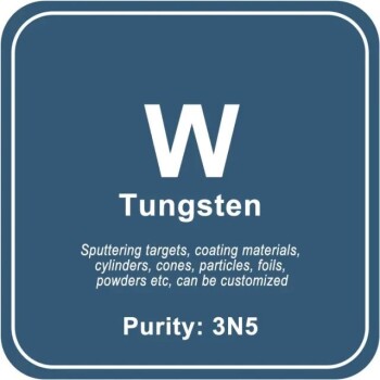
High Purity Tungsten (W) Sputtering Target / Powder / Wire / Block / Granule
Find high-quality Tungsten (W) materials for your laboratory needs at affordable prices. We offer customized purities, shapes, and sizes of sputtering targets, coating materials, powders, and more.
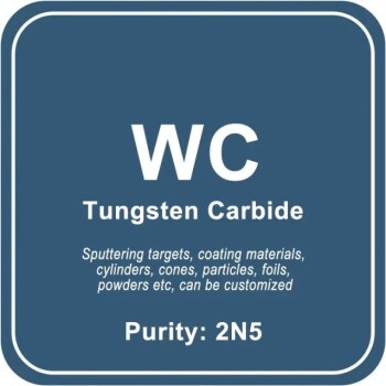
Tungsten Carbide (WC) Sputtering Target / Powder / Wire / Block / Granule
Looking for affordable Tungsten Carbide (WC) materials for your lab? Our expertly tailored products come in various shapes and sizes, from sputtering targets to nanometer powders. Shop now for quality materials that fit your unique needs.
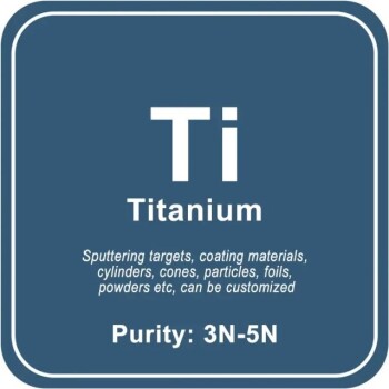
High Purity Titanium (Ti) Sputtering Target / Powder / Wire / Block / Granule
Shop for high-quality Titanium (Ti) materials at reasonable prices for laboratory use. Find a wide range of tailored products to suit your unique needs, including sputtering targets, coatings, powders, and more.
Tantalum Tungsten Alloy (TaW) Sputtering Target / Powder / Wire / Block / Granule
Looking for high-quality Tantalum Tungsten Alloy (TaW) materials? We offer a wide range of customizable options at competitive prices for laboratory use, including sputtering targets, coatings, powders, and more.
Titanium Carbide (TiC) Sputtering Target / Powder / Wire / Block / Granule
Get high-quality Titanium Carbide (TiC) materials for your lab at affordable prices. We offer a wide range of shapes and sizes, including sputtering targets, powders, and more. Tailored to your specific needs.
Titanium Nickel Silver Alloy (TiNiAg) Sputtering Target / Powder / Wire / Block / Granule
Looking for customizable TiNiAg materials? We offer a wide range of sizes and purities at competitive prices, including sputtering targets, coating materials, powders, and more. Contact us today!

Tungsten Sulfide (WS2) Sputtering Target / Powder / Wire / Block / Granule
Looking for Tungsten Sulfide (WS2) materials for your lab? We offer a range of customizable options at great prices, including sputtering targets, coating materials, powders, and more. Order now!
High Purity Tungsten Oxide (WO3) Sputtering Target / Powder / Wire / Block / Granule
Looking for high-quality Tungsten Oxide (WO3) materials? Our laboratory-grade products are tailored to your specific needs, with a range of purities, shapes, and sizes available. Shop sputtering targets, coating materials, and more.
Titanium Silicon Alloy (TiSi) Sputtering Target / Powder / Wire / Block / Granule
Discover our affordable Titanium Silicon Alloy (TiSi) materials for laboratory use. Our custom production offers various purities, shapes, and sizes for sputtering targets, coatings, powders, and more. Find the perfect match for your unique needs.
Titanium Nitride (TiN) Sputtering Target / Powder / Wire / Block / Granule
Looking for affordable Titanium Nitride (TiN) materials for your lab? Our expertise lies in producing tailored materials of different shapes and sizes to meet your unique needs. We offer a wide range of specifications and sizes for sputtering targets, coatings, and more.
Lithium Titanate (Li2TiO3) Sputtering Target / Powder / Wire / Block / Granule
Get high-quality Lithium Titanate materials for your lab needs at affordable prices. We offer tailored solutions with different shapes, sizes, and purities. Find sputtering targets, powders, and more in various specifications.
High Purity Titanium Dioxide (TiO2) Sputtering Target / Powder / Wire / Block / Granule
Looking for high-quality Titanium Dioxide materials? Our tailored products suit any lab's unique requirements. Browse our range of shapes, sizes, and purities today.
Chromium Nickel Alloy (CrNi) Sputtering Target / Powder / Wire / Block / Granule
Looking for high-quality Chromium Nickel Alloy (CrNi) materials for your lab? Look no further than our expertly crafted and tailored options. Explore our wide range of sizes and specifications, including sputtering targets, coatings, powders, and more. Shop now!
Iithium titanate (LiTiO3) Sputtering Target / Powder / Wire / Block / Granule
Get high-quality Iithium Titanate (LiTiO3) materials for your laboratory at reasonable prices. Our tailored solutions cater to different purities, shapes, and sizes, including sputtering targets, coating materials, powders, and more. Order now!
Nickel Chromium Alloy (NiCr) Sputtering Target / Powder / Wire / Block / Granule
Get high-quality Nickel Chromium Alloy (NiCr) materials for your lab needs at affordable prices. Choose from a wide range of shapes and sizes, including sputtering targets, coatings, powders, and more. Tailored to suit your unique requirements.
Thermally evaporated tungsten wire
It has a high melting point, thermal and electrical conductivity, and corrosion resistance. It is a valuable material for high temperature, vacuum and other industries.
Related Articles

Exploring the Benefits of Using Tungsten for Furnace Heating
Tungsten has a number of properties that make it well-suited for use in high-temperature furnaces.
Exploring the Capabilities and Applications of Warm Isostatic Pressing (WIP)
Dive into the comprehensive guide on Warm Isostatic Pressing (WIP), its technology, applications, and benefits in material processing. Discover how WIP enhances material properties and its role in advanced manufacturing.
Warm Isostatic Pressing for High-Density and Low-Defect Materials
Warm Isostatic Pressing (WIP) is a high-pressure technique used to enhance the density and reduce the defects of materials. It involves subjecting a material to high pressure and high temperature while simultaneously applying an inert gas, which uniformly compresses the material.
How To Turn XRF analysis sample preparation Into Success
In X-ray fluorescence (XRF) analysis, sample preparation is an important step because it can significantly impact both the quality and the efficiency of the analysis.
An In-depth Study of Isostatic Presses: Types, Applications, and Advantages
Isostatic presses play a crucial role in various industries, offering unique capabilities for material consolidation and product creation. These powerful machines apply equal pressure from all directions, resulting in products with uniform density and reduced defects. Isostatic presses are divided into two main types: Cold Isostatic Presses (CIP) and Hot Isostatic Presses (HIP). Each type functions under different conditions, allowing for a wide range of applications.
An In-depth Analysis of Cold Isostatic Pressing Services
Cold isostatic pressing (CIP) services utilize extremely high pressures to sterilize products or cold compact powders. CIP is particularly effective in producing complex shapes and increasing the final density of materials.
How to Ensure Molding Quality and Efficiency with Warm Isostatic Press
Warm Isostatic Press (WIP) is a type of isostatic press that uses a combination of heat and pressure to create high-quality parts. The WIP process involves placing a part inside a flexible mold, which is then filled with a gas or liquid media.
Manufacturing Sputtering Targets Using Powder Metallurgy
Detailed process and applications of powder metallurgy in manufacturing sputtering targets.
Introduction to Sputtering Targets
An overview of sputtering targets, their types, and key parameters like purity, density, and grain size.
Advanced Surface Treatment: Titanium CVD Coating
Explores the benefits and applications of CVD coatings on titanium alloys, focusing on wear resistance, corrosion resistance, and thermal stability.
High-Purity Sputtering Targets for Integrated Circuit Manufacturing
This article discusses the high-purity requirements and applications of various sputtering targets in integrated circuit manufacturing, focusing on metals and alloys used in different technology nodes.
Challenges in the Development and Application of Tantalum in Vacuum Deposition Equipment
This article discusses the role of tantalum in vacuum deposition equipment, focusing on its properties, manufacturing challenges, and its critical applications in industries like OLED screen production.