Lab Materials
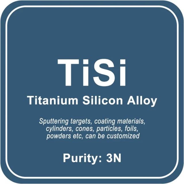
Titanium Silicon Alloy (TiSi) Sputtering Target / Powder / Wire / Block / Granule
Item Number : LM-TiSi
Price varies based on specs and customizations
- Chemical Formula
- TiSi
- Purity
- 3N
- Commonly used ratio
- Ti:Si= 1:2 at%
- Shape
- discs / wire / block / powder / plates / column targets / step target / custom-made

Shipping:
Contact us to get shipping details Enjoy On-time Dispatch Guarantee.
Ingredient Quality Control
- Raw material composition analysis
- Through the use of equipment such as ICP and GDMS, the content of metal impurities is detected and analyzed to ensure that it meets the purity standard;
Non-metallic impurities are detected by equipment such as carbon and sulfur analyzers, nitrogen and oxygen analyzers. - Metallographic flaw detection analysis
- The target material is inspected using flaw detection equipment to ensure that there are no defects or shrinkage holes inside the product;
Through metallographic testing, the internal grain structure of the target material is analyzed to ensure that the grains are fine and dense. - Appearance and dimension inspection
- Product dimensions are measured using micrometers and precision calipers to ensure compliance with drawings;
The surface finish and cleanliness of the product are measured using a surface cleanliness meter.
Conventional Sputtering Target Sizes
- Preparation process
- hot isostatic pressing, vacuum melting, etc.
- Sputtering target shape
- plane sputtering target, multi-arc sputtering target, step sputtering target, special-shaped sputtering target
- Round sputtering target size
- Diameter: 25.4mm / 50mm / 50.8mm / 60mm / 76.2mm / 80mm / 100mm / 101.6mm / 152.4mm
Thickness: 3mm / 4mm / 5mm / 6mm / 6.35mm
Size can be customized. - Square sputtering target size
- 50×50×3mm / 100×100×4mm / 300×300×5mm, size can be customized
Available Metal Forms
Metal Forms Details
We manufacture almost all the metals listed on the periodic table in a wide range of forms and purities, as well as standard sizes and dimensions. We can also produce custom-made products to meet specific customer requirements, such as size, shape, surface area, composition, and more. The following list provides a sample of the forms we offer, but it is not exhaustive. If you need laboratory consumables, please contact us directly to request a quote.
- Flat/Planar Forms: Board, Film, Foil, Microfoil, Microleaf, Paper, Plate, Ribbon, Sheet, Strip, Tape, Wafer
- Preformed Shapes: Anodes, Balls, Bands, Bars, Boats, Bolts, Briquettes, Cathodes, Circles, Coils, Crucibles, Crystals, Cubes, Cups, Cylinders, Discs, Electrodes, Fibers, Filaments, Flanges, Grids, Lenses, Mandrels, Nuts, Parts, Prisms, Pucks, Rings, Rods, Shapes, Shields, Sleeves, Springs, Squares, Sputtering Targets, Sticks, Tubes, Washers, Windows, Wires
- Microsizes: Beads, Bits, Capsules, Chips, Coins, Dust, Flakes, Grains, Granules, Micropowder, Needles, Particles, Pebbles, Pellets, Pins, Pills, Powder, Shavings, Shot, Slugs, Spheres, Tablets
- Macrosizes: Billets, Chunks, Cuttings, Fragments, Ingots, Lumps, Nuggets, Pieces, Punchings, Rocks, Scraps, Segments, Turnings
- Porous and Semi-Porous: Fabric, Foam, Gauze, Honeycomb, Mesh, Sponge, Wool
- Nanoscale: Nanoparticles, Nanopowders, Nanofoils, Nanotubes, Nanorods, Nanoprisms
- Others: Concentrate, Ink, Paste, Precipitate, Residue, Samples, Specimens
KinTek specializes in the manufacturing of high-purity and ultra-high-purity materials with a purity range of 99.999% (5N), 99.9999% (6N), 99.99995% (6N5), and in some cases, up to 99.99999% (7N). Our materials are available in specific grades, including UP/UHP, semiconductor, electronic, deposition, fiber optic, and MBE grades. Our high-purity metals, oxides, and compounds are specifically crafted to meet the rigorous demands of high-technology applications and are ideal for use as dopants and precursor materials for thin film deposition, crystal growth of semiconductors, and synthesis of nanomaterials. These materials find use in advanced microelectronics, solar cells, fuel cells, optical materials, and other cutting-edge applications.
Packaging
We use vacuum packaging for our high-purity materials, and each material has specific packaging tailored to its unique characteristics. For instance, our Hf sputter target is externally tagged and labeled to facilitate efficient identification and quality control. We take great care to prevent any damage that could occur during storage or transportation.
FAQ
What Is Sputtering Target?
What Are High Purity Materials?
How Are Sputtering Targets Made?
What Is Sputtering Target Used For?
What Are Sputtering Targets For Electronics?
What Is The Lifetime Of A Sputtering Target?
4.8
out of
5
KINTEK SOLUTION's TiSi Sputtering Target offers exceptional quality at a competitive price. The customizable options for purity, shape, and size make it an excellent choice for various applications.
4.9
out of
5
I'm impressed with the purity and consistency of KINTEK SOLUTION's TiSi materials. They have consistently met our strict quality standards, making them a reliable partner for our research.
4.7
out of
5
The Titanium Silicon Alloy from KINTEK SOLUTION has proven to be a valuable addition to our lab. Its versatility and availability in various forms have made it a go-to material for multiple projects.
4.9
out of
5
Working with KINTEK SOLUTION has been a pleasure. Their expertise in tailoring TiSi materials to our specific requirements has enabled us to achieve exceptional results in our research.
4.6
out of
5
KINTEK SOLUTION's TiSi Sputtering Target has significantly improved the quality of our thin films. The low particle counts have resulted in smoother and more uniform coatings.
4.8
out of
5
The customizable packaging options offered by KINTEK SOLUTION are a lifesaver. We can easily receive TiSi in forms that perfectly suit our experimental setups, saving us time and resources.
4.7
out of
5
The Titanium Silicon Alloy from KINTEK SOLUTION has proven to be a reliable material for our CVD and PVD applications. Its consistent quality ensures repeatable and successful experiments.
4.9
out of
5
KINTEK SOLUTION's TiSi Sputtering Target has enabled us to achieve exceptional results in our research. The high purity and fine grain structure have contributed to the superior performance of our devices.
4.6
out of
5
The technical support provided by KINTEK SOLUTION is outstanding. Their experts have guided us through every step of the process, ensuring successful implementation of TiSi materials in our laboratory.
4.8
out of
5
KINTEK SOLUTION's TiSi materials have met all our expectations. The fast delivery and responsive customer service have made working with them a seamless and enjoyable experience.
4.7
out of
5
The Titanium Silicon Alloy from KINTEK SOLUTION has proven to be a cost-effective option for our research. Its durability and longevity have reduced our material consumption and saved us money.
4.9
out of
5
The technological advancements incorporated into KINTEK SOLUTION's TiSi materials have enabled us to explore new possibilities in our research. Their commitment to innovation is truly commendable.
4.6
out of
5
I highly recommend KINTEK SOLUTION for their reliable and high-quality TiSi materials. Their products have consistently met our stringent requirements, making them an invaluable asset to our laboratory.
REQUEST A QUOTE
Our professional team will reply to you within one business day. Please feel free to contact us!
Related Products
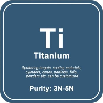
High Purity Titanium (Ti) Sputtering Target / Powder / Wire / Block / Granule
Shop for high-quality Titanium (Ti) materials at reasonable prices for laboratory use. Find a wide range of tailored products to suit your unique needs, including sputtering targets, coatings, powders, and more.
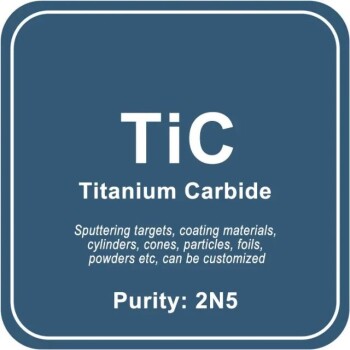
Titanium Carbide (TiC) Sputtering Target / Powder / Wire / Block / Granule
Get high-quality Titanium Carbide (TiC) materials for your lab at affordable prices. We offer a wide range of shapes and sizes, including sputtering targets, powders, and more. Tailored to your specific needs.
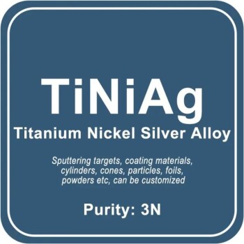
Titanium Nickel Silver Alloy (TiNiAg) Sputtering Target / Powder / Wire / Block / Granule
Looking for customizable TiNiAg materials? We offer a wide range of sizes and purities at competitive prices, including sputtering targets, coating materials, powders, and more. Contact us today!
Tungsten Titanium Alloy (WTi) Sputtering Target / Powder / Wire / Block / Granule
Discover our Tungsten Titanium Alloy (WTi) materials for laboratory use at affordable prices. Our expertise allows us to produce custom materials of different purities, shapes, and sizes. Choose from a wide range of sputtering targets, powders, and more.
Titanium Nitride (TiN) Sputtering Target / Powder / Wire / Block / Granule
Looking for affordable Titanium Nitride (TiN) materials for your lab? Our expertise lies in producing tailored materials of different shapes and sizes to meet your unique needs. We offer a wide range of specifications and sizes for sputtering targets, coatings, and more.
High Purity Titanium Dioxide (TiO2) Sputtering Target / Powder / Wire / Block / Granule
Looking for high-quality Titanium Dioxide materials? Our tailored products suit any lab's unique requirements. Browse our range of shapes, sizes, and purities today.
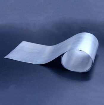
High-purity titanium foil / titanium sheet
Titanium is chemically stable, with a density of 4.51g/cm3, which is higher than aluminum and lower than steel, copper, and nickel, but its specific strength ranks first among metals.
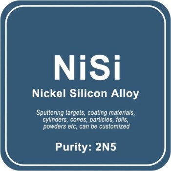
Nickel Silicon Alloy (NiSi) Sputtering Target / Powder / Wire / Block / Granule
Looking for Nickel Silicon Alloy materials for your lab? Our expertly produced and tailored materials come in various shapes and sizes to suit your unique needs. Get sputtering targets, coating materials, powders, and more at reasonable prices.

Aluminum-plastic flexible packaging film for lithium battery packaging
Aluminum-plastic film has excellent electrolyte properties and is an important safe material for soft-pack lithium batteries. Unlike metal case batteries, pouch batteries wrapped in this film are safer.
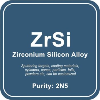
Zirconium Silicon Alloy (ZrSi) Sputtering Target / Powder / Wire / Block / Granule
Discover our Zirconium Silicon Alloy (ZrSi) materials for laboratory use at affordable prices. We produce tailored materials to fit your unique requirements, offering a wide range of specifications and sizes for sputtering targets, coating materials, powders, and more.
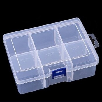
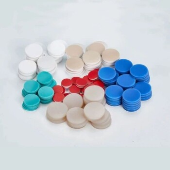
Button-type battery storage box, detachable, high-quality PP environmental protection material; suitable for small objects/chemicals, etc., thickened, compressive, durable, and available in a variety of styles.
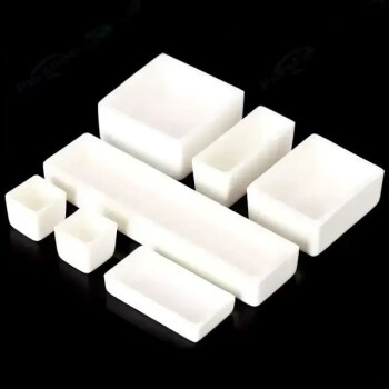
PTFE container is a container with excellent corrosion resistance and chemical inertness.
Lithium Titanate (Li2TiO3) Sputtering Target / Powder / Wire / Block / Granule
Get high-quality Lithium Titanate materials for your lab needs at affordable prices. We offer tailored solutions with different shapes, sizes, and purities. Find sputtering targets, powders, and more in various specifications.
PTFE acid and alkali resistant scoops/chemical powder material scoops
Known for its excellent thermal stability, chemical resistance and electrical insulating properties, PTFE is a versatile thermoplastic material.
High Purity Tantalum (Ta) Sputtering Target / Powder / Wire / Block / Granule
Discover our high-quality Tantalum (Ta) materials for laboratory use at affordable prices. We tailor to your specific requirements with various shapes, sizes, and purities. Explore our range of sputtering targets, coating materials, powders, and more.
High Purity Silicon (Si) Sputtering Target / Powder / Wire / Block / Granule
Looking for high-quality Silicon (Si) materials for your laboratory? Look no further! Our custom-produced Silicon (Si) materials come in various purities, shapes, and sizes to suit your unique requirements. Browse our selection of sputtering targets, powders, foils, and more. Order now!
Aluminum foil current collector for lithium battery
The surface of aluminum foil is extremely clean and hygienic, and no bacteria or microorganisms can grow on it. It is a non-toxic, tasteless and plastic packaging material.
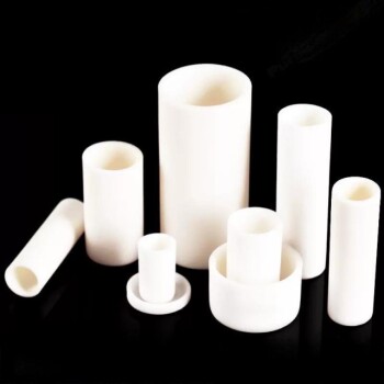
Alumina (Al2O3) Crucible With Lid Cylindrical Laboratory Crucible
Cylindrical Crucibles Cylindrical crucibles are one of the most common crucible shapes, suitable for melting and processing a wide variety of materials, and are easy to handle and clean.
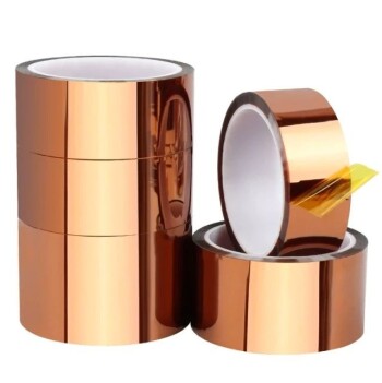
PI polyimide tape, generally brown, also known as gold finger tape, high temperature resistance 280 ℃, to prevent the influence of heat sealing of soft pack battery lug glue, suitable for soft pack battery tab position glue.
Tantalum Tungsten Alloy (TaW) Sputtering Target / Powder / Wire / Block / Granule
Looking for high-quality Tantalum Tungsten Alloy (TaW) materials? We offer a wide range of customizable options at competitive prices for laboratory use, including sputtering targets, coatings, powders, and more.
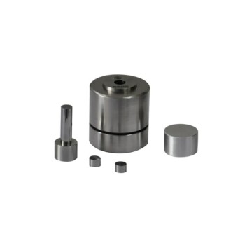
Assemble Lab Cylindrical Press Mold
Get reliable and precise molding with Assemble Lab Cylindrical Press Mold. Perfect for ultra-fine powder or delicate samples, widely used in material research and development.

High Purity Tellurium (Te) Sputtering Target / Powder / Wire / Block / Granule
Discover our range of high-quality Tellurium (Te) materials for laboratory use at affordable prices. Our expert team produces custom sizes and purities to fit your unique needs. Shop sputtering targets, powders, ingots, and more.
Gaskets are materials placed between two flat surfaces to enhance the seal. To prevent fluid leakage, sealing elements are arranged between static sealing surfaces.
Alumina (Al2O3) Ceramic Crucible For Laboratory Muffle Furnace
Alumina ceramic crucibles are used in some materials and metal melting tools, and flat-bottomed crucibles are suitable for melting and processing larger batches of materials with better stability and uniformity.
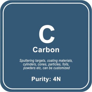
High Purity Carbon (C) Sputtering Target / Powder / Wire / Block / Granule
Looking for affordable Carbon (C) materials for your laboratory needs? Look no further! Our expertly produced and tailored materials come in a variety of shapes, sizes, and purities. Choose from sputtering targets, coating materials, powders, and more.

Conductive Carbon Cloth / Carbon Paper / Carbon Felt
Conductive carbon cloth, paper, and felt for electrochemical experiments. High-quality materials for reliable and accurate results. Order now for customization options.
Related Articles

An In-depth Analysis of Cold Isostatic Pressing Services
Cold isostatic pressing (CIP) services utilize extremely high pressures to sterilize products or cold compact powders. CIP is particularly effective in producing complex shapes and increasing the final density of materials.
Detailed Processes and Parameters of PECVD for TiN and Si3N4 Deposition
An in-depth exploration of the PECVD processes for TiN and Si3N4, including equipment setup, operational steps, and key process parameters.
Advanced Surface Treatment: Titanium CVD Coating
Explores the benefits and applications of CVD coatings on titanium alloys, focusing on wear resistance, corrosion resistance, and thermal stability.
Carbon Coating for Surface Modification of Silicon-Based Materials in Lithium-Ion Batteries
This article discusses the application of carbon coatings to improve the performance of silicon-based anode materials in lithium-ion batteries.
Analysis of Severe Ablation in the Center Region of Ceramic Targets in Magnetron Sputtering
This article discusses the causes and solutions for severe ablation in the center region of ceramic targets during magnetron sputtering.
PVD Sputtering Targets and Hot Isostatic Pressing: Part 1
Explores the use of hot isostatic pressing in producing high-quality sputtering targets and the applications of PVD sputtering technology.
Controlling Color and Applications of Evaporated Silicon Oxide Films
Exploring color variation, control methods, and practical applications of silicon oxide thin films.