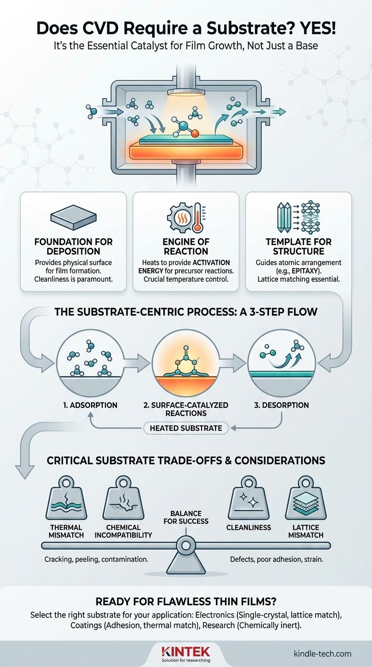
Yes, Chemical Vapor Deposition (CVD) fundamentally requires a substrate. The substrate is not merely a passive carrier for the final product; it is the active and essential surface where the entire deposition process takes place. It provides the physical foundation and the necessary thermal energy that drives the conversion of gas-phase chemicals into a solid thin film.
The substrate in a CVD process is the essential catalyst for film growth. It provides the necessary surface and thermal energy to convert volatile precursor gases into a solid, high-performance film, directly controlling the final material's structure and quality.
The Substrate's Role: More Than Just a Surface
To understand why the substrate is non-negotiable, we must look beyond its role as a simple base. It is an active participant in the chemical and physical transformations that define the CVD process.
The Foundation for Deposition
At its most basic level, the substrate provides the physical location for film formation. The goal of CVD is to create a coherent, solid layer of material, and this layer must be deposited onto something.
The Engine of Reaction
In most CVD processes, the substrate is heated to a specific, high temperature. This heat is not just for warming the environment; it provides the critical activation energy required for the precursor gases to react or decompose on the surface. The substrate's temperature is one of the most important control parameters of the entire process.
The Template for Structure
The substrate's own physical structure can directly influence the structure of the film being grown. For high-performance applications like semiconductors, a single-crystal substrate (like a silicon wafer) is used to guide the deposited atoms into a perfectly ordered, single-crystal film in a process called epitaxy.
How CVD Works: A Substrate-Centric Process
The sequence of events in CVD highlights the substrate's central role at every critical stage. The process fails if any of these substrate-dependent steps are compromised.
Adsorption of Precursors
First, the reactant gases (precursors) must physically attach to the substrate's surface. This step, known as adsorption, brings the molecules into direct contact with the heated surface where the reaction will occur.
Surface-Catalyzed Reactions
This is the heart of CVD. The thermal energy from the substrate drives the desired chemical reactions. This heterogeneous reaction (occurring at the gas-solid interface) is what builds the film layer by layer. The alternative, a homogeneous reaction (occurring in the gas phase), creates unwanted dust particles instead of a quality film.
Desorption of Byproducts
As the precursors react to form the solid film, gaseous byproducts are created. These byproducts must detach from the surface (desorption) and be exhausted from the chamber to allow new reactants to reach the surface and continue the growth process.
Understanding the Trade-offs: Substrate Selection is Critical
Choosing the wrong substrate or preparing it improperly is a common source of failure in CVD. The interaction between the film and the substrate introduces several critical trade-offs.
Thermal Mismatch
If the substrate and the film have significantly different rates of thermal expansion, the film can crack or peel off the substrate as it cools down from the high deposition temperature. This is a catastrophic failure mode.
Chemical Incompatibility
The substrate must be chemically stable at high temperatures and in the presence of the reactive precursor gases. An unstable substrate can corrode or unintentionally participate in the chemical reaction, contaminating the film.
The Critical Need for Cleanliness
Any microscopic dust particle, organic residue, or native oxide layer on the substrate surface will disrupt the film's growth. This leads to defects, poor adhesion, and compromised material properties. Substrate cleaning is an absolutely vital preparatory step.
Lattice Mismatch in Epitaxy
For single-crystal films, the atomic spacing of the substrate's crystal lattice must closely match that of the desired film. A significant mismatch introduces strain and crystal defects, degrading the electronic or optical performance of the final device.
Making the Right Choice for Your Goal
The ideal substrate is always defined by the intended application of the final film. Your selection process must balance chemical, thermal, and structural requirements.
- If your primary focus is producing high-performance electronics: You must use a single-crystal substrate, like a silicon wafer, with precise lattice matching to achieve the required epitaxial film quality.
- If your primary focus is creating a hard, protective coating: Your priority is a substrate material with excellent adhesion properties and a thermal expansion coefficient similar to the coating to prevent cracking under stress.
- If your primary focus is fundamental materials research: Select a substrate that is chemically inert to your process, such as sapphire or quartz, to ensure the properties you measure belong to your film, not an interaction with the substrate.
Ultimately, treating the substrate as an active component of the reaction, not just a passive carrier, is the key to mastering the CVD process and achieving reliable, high-quality results.
Summary Table:
| Substrate Function | Impact on CVD Process | Key Consideration |
|---|---|---|
| Foundation for Deposition | Provides the physical surface for film formation. | Surface cleanliness is paramount. |
| Engine of Reaction | Heated to provide activation energy for precursor reactions. | Temperature control is critical. |
| Template for Structure | Guides atomic arrangement (e.g., epitaxial growth). | Lattice matching is essential for single-crystal films. |
| Determines Adhesion | Influences film stability and resistance to peeling/cracking. | Thermal expansion coefficient must be compatible. |
Ready to achieve flawless thin films with your CVD process? The foundation of your success starts with the right substrate and process expertise. At KINTEK, we specialize in providing high-quality lab equipment and consumables tailored to your specific laboratory needs. Whether you are developing advanced semiconductors, durable coatings, or conducting cutting-edge materials research, our team can help you select the optimal setup for superior results.
Contact KINTEK today to discuss how we can support your project and ensure your substrate choice leads to a perfect deposition every time.
Visual Guide
Related Products
- Conductive Carbon Cloth Carbon Paper Carbon Felt for Electrodes and Batteries
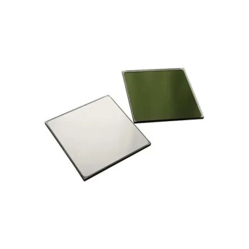
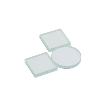
- Optical Window Glass Substrate Wafer Quartz Plate JGS1 JGS2 JGS3
- CVD Diamond for Thermal Management Applications
- Laboratory CVD Boron Doped Diamond Materials
- MgF2 Magnesium Fluoride Crystal Substrate Window for Optical Applications
People Also Ask
- What are carbon cloths used for? Conquer Static Dust on Electronics & Screens
- What is a critical step when using carbon felt in an experiment? Ensure Complete Saturation for Maximum Efficiency
- What are the examples of electrode materials? From Platinum to Graphite for Your Application
- What are the common applications for carbon cloth? Unlock Its Potential in Energy & Electrochemical Systems
- How can the flexibility of carbon cloth be maintained over time? Preserve Mechanical Integrity with NAFION