In essence, thin films are created by depositing material onto a surface, known as a substrate, in a highly controlled manner. These deposition processes are sophisticated enough to build films layer by layer, sometimes even one atom at a time. The methods fall into two primary categories: physical techniques that transfer a solid material through a vacuum, and chemical techniques that use reactions to form the film on the substrate.
The fundamental choice in thin film manufacturing is between Physical Vapor Deposition (PVD) and Chemical Deposition. PVD physically moves material from a source to a substrate, while Chemical Deposition uses a chemical reaction on the substrate's surface to grow the film. Your end goal—be it precision, cost, or specific material properties—will dictate which method is appropriate.
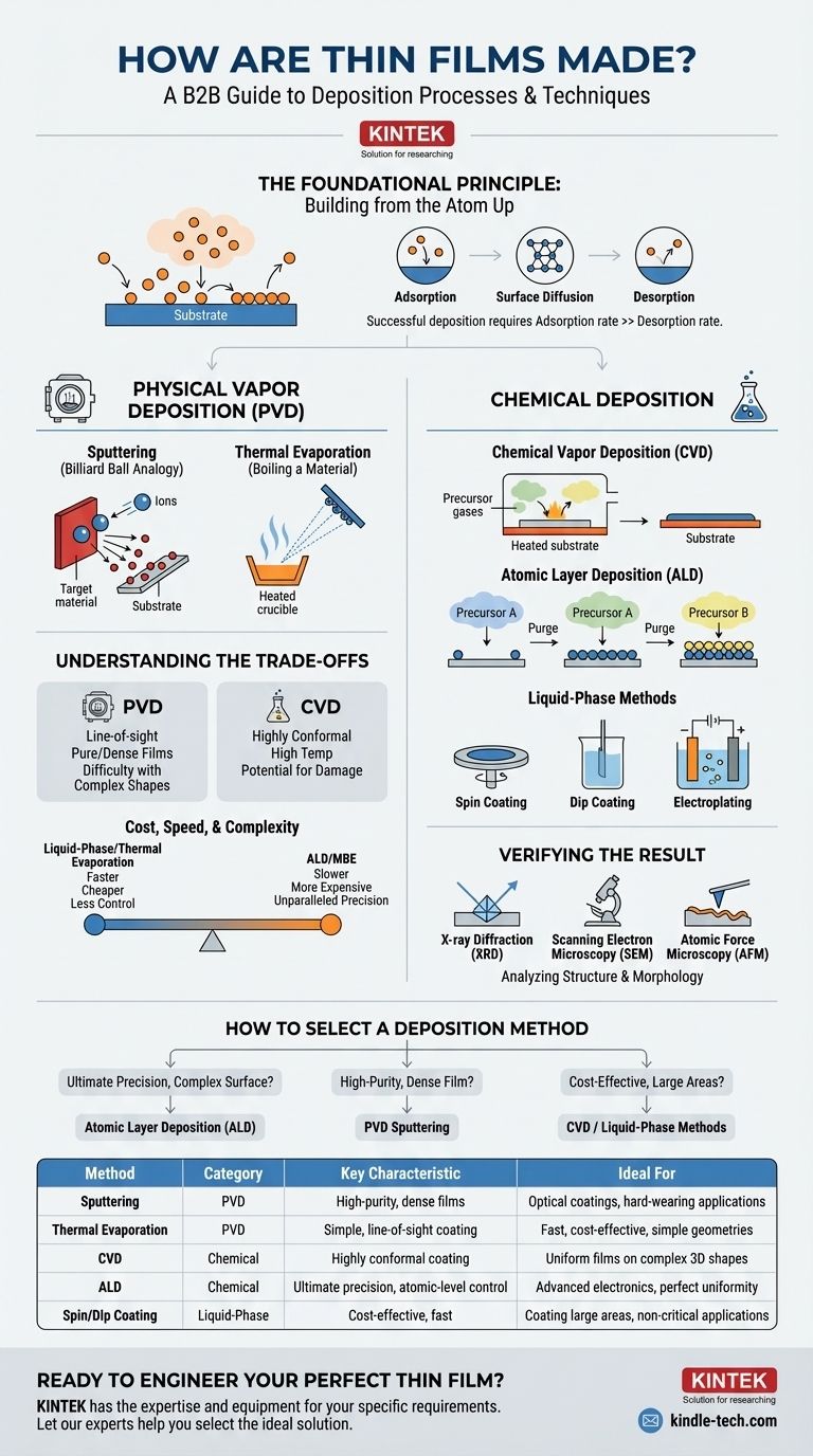
The Foundational Principle: Building from the Atom Up
Before examining specific techniques, it's critical to understand the universal process that governs how any thin film forms. This process is a delicate balance of three atomic-scale events.
Adsorption
This is the initial step where atoms or molecules from a gas or liquid stick to the substrate's surface. For a film to form, the particles must successfully land and stay on the surface.
Surface Diffusion
Once adsorbed onto the surface, atoms are not necessarily static. They can move around, or "diffuse," across the surface until they find a stable, low-energy position, often bonding with other atoms to begin forming the film's crystal structure.
Desorption
Desorption is the opposite of adsorption; it's the process by which a previously adsorbed atom leaves the surface. A successful deposition process requires the rate of adsorption to be significantly higher than the rate of desorption.
Category 1: Physical Vapor Deposition (PVD)
Physical Vapor Deposition encompasses a family of techniques that occur in a vacuum. The core principle involves taking a solid source material, turning it into a vapor, and having it condense on the substrate to form the film.
Sputtering: A Billiard Ball Analogy
Sputtering is a widely used PVD method. In this process, high-energy ions (typically from an inert gas like argon) are shot at a source material, called a target. These ions act like atomic-scale billiard balls, knocking atoms off the target, which then travel through the vacuum and coat the substrate.
Thermal Evaporation: Boiling a Material
This is one of the simplest PVD techniques. The source material is heated in a high vacuum until it evaporates or sublimes. This vapor then travels in a straight line until it condenses on the cooler substrate, forming the film.
Category 2: Chemical Deposition
Unlike PVD, chemical deposition methods do not physically transfer the final film material. Instead, they introduce precursor chemicals that react on or near the substrate's surface to form the desired material.
Chemical Vapor Deposition (CVD)
In CVD, the substrate is placed in a reaction chamber and exposed to one or more volatile precursor gases. These gases react or decompose on the hot substrate surface, leaving behind a solid film. This method is excellent for coating complex shapes conformity.
Atomic Layer Deposition (ALD)
ALD is a variation of CVD that offers the ultimate control over film thickness and uniformity. It works by exposing the substrate to different precursor gases in sequential, self-limiting steps. This process builds the film one perfect atomic layer at a time, making it ideal for advanced electronics.
Liquid-Phase Methods: Coating and Plating
This broad sub-category includes techniques like spin coating, dip coating, and electroplating. These methods use a liquid containing the desired material or its chemical precursors, which is applied to the substrate and then solidified through drying, curing, or an electrochemical reaction.
Understanding the Trade-offs
No single deposition method is universally superior. The choice is a technical and economic decision based on a series of trade-offs.
PVD: Line-of-Sight Limitation
PVD methods are typically "line-of-sight," meaning the source material can only coat surfaces it can directly "see." This can make it difficult to uniformly coat complex, three-dimensional objects. However, PVD often produces very pure, dense films.
CVD: Conformance vs. Temperature
CVD excels at creating highly conformal films that uniformly coat intricate geometries. The primary drawback is that many CVD processes require very high substrate temperatures, which can damage sensitive components like polymers or previously fabricated electronic circuits.
Cost, Speed, and Complexity
Generally, liquid-phase methods and thermal evaporation are faster and less expensive but offer less control. Advanced techniques like Molecular Beam Epitaxy (MBE) or Atomic Layer Deposition (ALD) provide unparalleled precision but are slow, complex, and carry a significantly higher cost.
Verifying the Result: Characterizing the Film
Creating a film is only half the battle. Technicians must verify its properties to ensure it meets specifications.
Measuring Structure and Morphology
Techniques like X-ray Diffraction (XRD) are used to analyze the film's crystalline structure. To investigate the surface morphology—its smoothness, grain size, and physical features—engineers use powerful microscopy tools like Scanning Electron Microscopy (SEM) and Atomic Force Microscopy (AFM).
How to Select a Deposition Method
Your choice of method should be guided directly by your project's most critical requirement.
- If your primary focus is ultimate precision and perfect uniformity on a complex surface: Atomic Layer Deposition (ALD) is the superior choice.
- If your primary focus is a high-purity, dense film for optical or hard-wearing applications: Physical Vapor Deposition (PVD) methods like sputtering are often the industry standard.
- If your primary focus is cost-effective coating of large areas or non-flat parts: Chemical Vapor Deposition (CVD) or liquid-phase methods offer a compelling balance of performance and efficiency.
Understanding these fundamental deposition processes empowers you to engineer materials with precisely tailored properties for any application.
Summary Table:
| Deposition Method | Primary Category | Key Characteristic | Ideal For |
|---|---|---|---|
| Sputtering | Physical Vapor Deposition (PVD) | High-purity, dense films | Optical coatings, hard-wearing applications |
| Thermal Evaporation | Physical Vapor Deposition (PVD) | Simple, line-of-sight coating | Fast, cost-effective deposition on simple geometries |
| Chemical Vapor Deposition (CVD) | Chemical Deposition | Highly conformal coating | Uniform films on complex 3D shapes |
| Atomic Layer Deposition (ALD) | Chemical Deposition | Ultimate precision, atomic-level control | Advanced electronics, perfect uniformity |
| Spin/Dip Coating | Liquid-Phase Methods | Cost-effective, fast | Coating large areas, non-critical applications |
Ready to Engineer Your Perfect Thin Film?
Choosing the right deposition method is critical for your research and development. Whether you need the precision of ALD, the durability of PVD sputtering, or the conformal coverage of CVD, KINTEK has the expertise and equipment to meet your laboratory's specific requirements.
We specialize in providing high-quality lab equipment and consumables for all your thin film fabrication needs. Let our experts help you select the ideal solution to achieve precisely tailored material properties and accelerate your project's success.
Contact KINTEK today for a personalized consultation!
Visual Guide
Related Products
- Aluminized Ceramic Evaporation Boat for Thin Film Deposition
- Tungsten Evaporation Boat for Thin Film Deposition
- Electron Beam Evaporation Coating Oxygen-Free Copper Crucible and Evaporation Boat
- Molybdenum Tungsten Tantalum Evaporation Boat for High Temperature Applications
- Aluminum-Plastic Flexible Packaging Film for Lithium Battery Packaging
People Also Ask
- What is the widely used boat made of in thermal evaporation? Choosing the Right Material for High-Purity Deposition
- Why is an alumina boat selected for catalyst precursors? Ensure Sample Purity at 1000 °C
- What are thin films deposited by evaporation? A Guide to High-Purity Coating
- Why are high-purity ceramic boats used for lignin activation? Ensure Purity & Thermal Stability
- What is thin film deposition? Unlock Advanced Surface Engineering for Your Materials


