At its core, electron beam deposition is a physical vapor deposition (PVD) technique where an intense, focused beam of electrons heats a source material in a high-vacuum chamber. This energy causes the material to vaporize, and the resulting vapor travels through the vacuum to condense onto a cooler substrate, forming a highly pure and uniform thin film. This process is governed by precision computer control over factors like vacuum level, heating, and substrate rotation to achieve exact coating thicknesses.
The true value of electron beam deposition lies in its combination of speed, material flexibility, and precision. It excels at rapidly creating high-quality optical and polymeric coatings, offering a distinct advantage in high-volume commercial applications where both performance and cost-efficiency are critical.
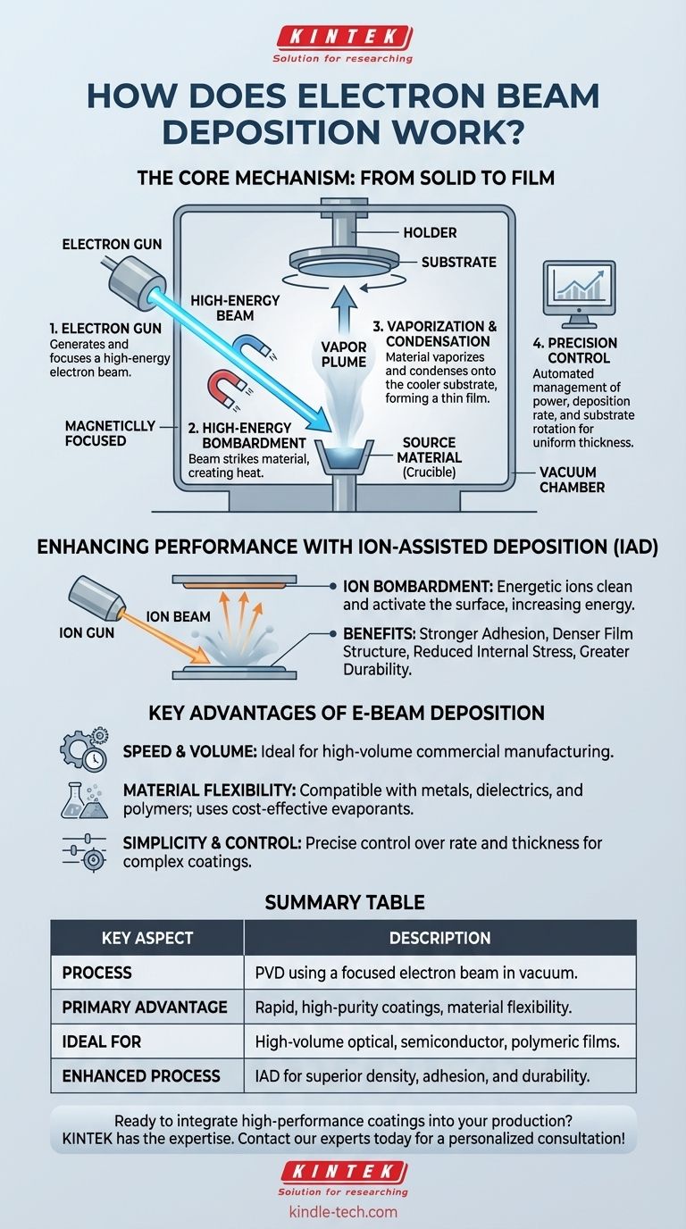
The Core Mechanism: From Solid to Film
To understand electron beam deposition, it's best to break it down into a sequence of distinct physical events that occur within the vacuum chamber.
The Electron Gun
The process begins with an electron gun, which generates a high-energy beam of electrons. This beam is then magnetically guided and focused with extreme precision onto a small crucible containing the source material you wish to deposit.
High-Energy Bombardment
Inside the high-vacuum environment, the focused electron beam strikes the source material—often in granular or powder form. The kinetic energy of the electrons is instantly converted into thermal energy, rapidly heating the material to its vaporization point.
Vaporization and Condensation
As the source material vaporizes, its atoms or molecules travel in a straight line through the vacuum. They eventually strike the cooler substrate (such as an optical lens or silicon wafer) that is strategically placed above the source. Upon contact, the vapor condenses back into a solid state, building up layer by layer to form a thin film.
Precision Control
The entire process is tightly controlled. Computers monitor and adjust the electron beam's power to manage the deposition rate, while the substrate is often rotated to ensure the final film has a uniform, pre-specified thickness across its entire surface.
Enhancing Performance with Ion-Assisted Deposition
For applications demanding superior film quality, the standard E-beam process can be augmented with an ion beam, a technique known as Ion-Assisted Deposition (IAD).
The Role of the Ion Beam
In an IAD setup, a separate ion gun bombards the substrate surface with energetic ions, typically before and during the deposition process.
Surface Activation and Cleaning
This ion bombardment serves a critical purpose: it cleans the substrate by sputtering away contaminants and increases the surface energy. This creates a highly activated surface that is much more receptive to the depositing material.
Denser, More Robust Films
The result is a significant improvement in film quality. The added energy from the ions leads to stronger adhesion, a denser film structure, and reduced internal stress. These coatings are more robust and durable than those produced by E-beam alone.
Understanding the Key Advantages
Electron beam deposition is not the only PVD method, but it holds several advantages that make it the preferred choice for specific applications, especially when compared to techniques like magnetron sputtering.
Advantage: Speed and Volume
E-beam deposition processes more rapidly in batch scenarios. This efficiency makes it an ideal solution for high-volume commercial manufacturing where throughput is a primary concern.
Advantage: Material Flexibility
The technique is compatible with a vast array of materials, including metals, dielectrics, and even polymers. The source materials, or evaporants, are often less expensive than the specialized targets required for magnetron sputtering.
Advantage: Simplicity and Control
While the physics is complex, the operational principle is relatively straightforward and flexible. It allows for precise control over the deposition rate and resulting film thickness, which is crucial for creating complex optical interference coatings.
Making the Right Choice for Your Goal
Selecting the right deposition technique depends entirely on your project's specific requirements for performance, material, and production volume.
- If your primary focus is high-volume optical coating manufacturing: E-beam deposition is a leading choice due to its rapid batch processing and material versatility.
- If your primary focus is achieving maximum film adhesion and durability: You should specify an E-beam process enhanced with Ion-Assisted Deposition (IAD).
- If your primary focus is cost-effective sourcing for a wide range of materials: E-beam's ability to use less expensive evaporants provides a significant economic advantage over target-based methods.
Ultimately, electron beam deposition offers a powerful and versatile tool for engineering precise, high-performance thin films at scale.
Summary Table:
| Key Aspect | Description |
|---|---|
| Process | Physical Vapor Deposition (PVD) using a focused electron beam to vaporize a source material in a vacuum. |
| Primary Advantage | Rapid deposition of high-purity coatings with excellent material flexibility. |
| Ideal For | High-volume manufacturing of optical coatings, semiconductor layers, and polymeric films. |
| Enhanced Process | Ion-Assisted Deposition (IAD) for superior film density, adhesion, and durability. |
Ready to integrate high-performance coatings into your production?
Electron beam deposition is a powerful solution for creating precise, high-purity thin films at scale. Whether your project requires rapid batch processing for optical components or the enhanced durability of Ion-Assisted Deposition, KINTEK has the expertise and equipment to meet your laboratory's specific needs.
Let's discuss how our lab equipment and consumables can optimize your thin film processes. Contact our experts today for a personalized consultation!
Visual Guide
Related Products
- Electron Beam Evaporation Coating Oxygen-Free Copper Crucible and Evaporation Boat
- RF PECVD System Radio Frequency Plasma-Enhanced Chemical Vapor Deposition RF PECVD
- Electron Beam Evaporation Coating Tungsten Crucible and Molybdenum Crucible for High Temperature Applications
- Electron Beam Evaporation Coating Conductive Boron Nitride Crucible BN Crucible
- Electron Beam Evaporation Coating Gold Plating Tungsten Molybdenum Crucible for Evaporation
People Also Ask
- How is an electron beam evaporator cooled during deposition? Essential Thermal Management for Stable Processes
- What is the container that holds the metal source material called in e-beam evaporation? Ensure Purity and Quality in Your Thin-Film Deposition
- What is e-beam evaporation used for? Precision Coating for Optics, Aerospace & Electronics
- What is e-beam evaporation? Achieve High-Purity Thin Film Deposition for Your Lab
- What is the current of e-beam evaporation? A Guide to High-Purity Thin Film Deposition


