At its core, Metal-Organic Chemical Vapor Deposition (MOCVD) is a highly-controlled process for building up ultra-thin, crystalline layers of material on a surface, atom by atom. It works by introducing volatile metal-organic precursor gases into a heated reaction chamber, where they decompose and deposit onto a substrate, forming a perfect, single-crystal film. This method is the cornerstone tecnologia for manufacturing high-performance light-emitting diodes (LEDs), lasers, and advanced RF components.
MOCVD is not merely a coating technique; it is a method of atomic-level construction. Its true value lies in its ability to grow complex, multi-layered crystalline structures with the extreme precision required for modern semiconductor devices.
The Core Principle: Building with Chemical Vapors
What is Chemical Vapor Deposition (CVD)?
Chemical Vapor Deposition is a family of processes used to create high-quality, solid thin films. The general principle involves placing a substrate, or wafer, inside a reaction chamber.
One or more volatile precursor gases are then introduced. Heat, and sometimes plasma, is applied to initiate a chemical reaction, causing a solid material to be extracted from the gas and "deposited" onto the wafer, layer by layer.
The "Metal-Organic" Distinction
MOCVD is a specific type of CVD. Its name comes from its unique precursors: metal-organic compounds.
These are specially designed molecules where a metal atom (like gallium, indium, or aluminum) is chemically bonded to organic molecules. These precursors are often liquids at room temperature, which makes them easier to handle and vaporize into a gas for the process.
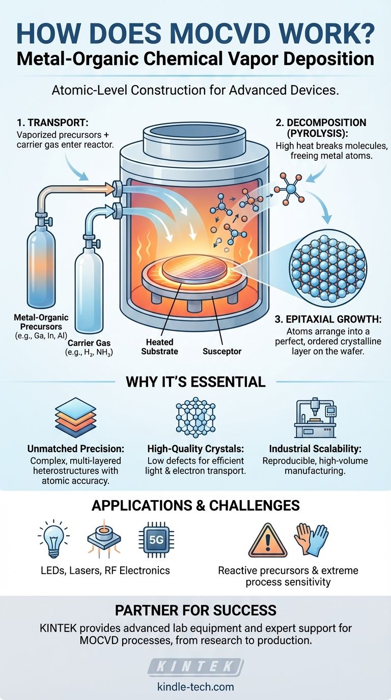
The MOCVD Process Step-by-Step
The process is a finely tuned sequence of events controlled by a sophisticated system.
- Transport: The liquid metal-organic precursors are vaporized and, along with other necessary gases (like ammonia for providing nitrogen), are carried into the reactor chamber by a carrier gas (e.g., hydrogen).
- Decomposition: Inside the hot chamber, the high temperatures cause the metal-organic molecules to break apart, a process known as pyrolysis. This frees the desired metal atoms.
- Epitaxial Growth: These freed metal and other atoms migrate to the heated substrate surface. They then arrange themselves in a highly ordered fashion that mirrors the underlying crystal structure of the wafer.
This layer-by-layer continuation of a crystal structure is called epitaxy. Because it is a vapor-phase process, MOCVD is also frequently referred to as Metal-Organic Vapor Phase Epitaxy (MOVPE).
Why MOCVD Is Essential for Compound Semiconductors
Unmatched Precision for Complex Layers
Modern devices like blue LEDs or semiconductor lasers are not made from a single material. They are heterostructures, built from a stack of dozens of different, ultra-thin semiconductor layers.
MOCVD excels at this. By simply switching the precursor gases flowing into the reactor, engineers can create atomically sharp transitions between layers, tailoring the electronic and optical properties of the device.
High-Quality Crystalline Growth
The performance of an LED or a laser is directly tied to the perfection of its crystal structure. Defects in the crystal act as traps that kill efficiency.
MOCVD produces films that are highly stoichiometric (having the correct ratio of chemical elements) and dense. This results in the high-purity, low-defect crystals电压 that are essential for efficient light generation and electron transport.
Industrial Scalability and Control
While the principles are complex, MOCVD equipment is highly automated. Advanced control systems manage gas flows, temperatures, and pressures with extreme precision.
This allows for the highly reproducible and high-volume manufacturing processos required to produce millions of LED chips and other semiconductor devices reliably.
Understanding the Trade-offs
Precursor Handling and Safety
The metal-organic precursors are the heart of the process, but they can also be its biggest challenge. They are often highly reactive, pyrophoric (ignite spontaneously in air), and toxic.
While modern liquid precursors are significantly safer than older compounds, njihovo rukovanje still requires stringent safety protocols and specialized equipment.
Extreme Process Sensitivity
The quality of the final crystalline film is incredibly sensitive to the process conditions. Minor fluctuations in temperature, pressure, or gas flow can introduce defects and ruin a device.
This is why MOCVD reactors are complex, expensive machines that require constant monitoring, calibration, and expert operation to maintain peak performance.
A Tool for a Specific Job
MOCVD is a powerful but specialized technique. Its primary strength is in creating a perfect, single-crystal epitaxial film.
For applications that only require a simple, non-crystalline (amorphous) coating, other simpler and more cost-effective methods like Physical Vapor Deposition (PVD) or other forms of CVD are often a better choice.
Making the Right Choice for Your Goal
MOCVD is the definitive choice when the atomic-level structure of the material dictates its function.
- If your primary focus is high-performance optoelectronics (LEDs, Lasers): MOCVD is the industry-standard technology, essential for creating the high-quality, multi-layered GaN heterostructures that produce light efficiently.
- If your primary focus is advanced RF electronics (e.g., 5G amplifiers): MOCVD is the key method for growing the III-V compound semiconductor layers (like GaN)订单 that enable high-power, high-frequency performance.
- If your primary focus is simple, durable thin-film coatings: A simpler deposition technique that does not require epitaxial growth, such as PVD or a basic CVD process, is likely a more practical and economical solution.
Ultimately, MOCVD is the precision engineering tool that enables us to build the foundational materials of modern photonic and electronic technology from the atom up.
Summary Table:
| Key Aspect | Description |
|---|---|
| Process Type | Chemical Vapor Deposition (CVD) with metal-organic precursors |
| Primary Use | Epitaxial growth of compound semiconductor layers |
| Key Applications | LEDs, Lasers, RF Electronics, High-Performance Semiconductors |
| Core Advantage | Atomic-level precision for complex multi-layer structures |
| Main Challenge | Precursor handling and extreme process sensitivity |
Ready to Advance Your Semiconductor Research?
MOCVD technology requires precision equipment and expert support to achieve optimal results. KINTEK specializes in advanced lab equipment and consumables for semiconductor manufacturing, serving research laboratories and production facilities worldwide.
Our team can help you:
- Select the right MOCVD system for your specific application
- Ensure proper handling of metal-organic precursors
- Maintain process consistency for high-quality epitaxial growth
- Scale your semiconductor development from research to production
Contact our semiconductor experts today to discuss how our solutions can enhance your MOCVD processes and accelerate your material development timeline.
Visual Guide
Related Products
- Multi Heating Zones CVD Tube Furnace Machine Chemical Vapor Deposition Chamber System Equipment
- 915MHz MPCVD Diamond Machine Microwave Plasma Chemical Vapor Deposition System Reactor
- Microwave Plasma Chemical Vapor Deposition MPCVD Machine System Reactor for Lab and Diamond Growth
- Cylindrical Resonator MPCVD Machine System Reactor for Microwave Plasma Chemical Vapor Deposition and Lab Diamond Growth
- Molybdenum Vacuum Heat Treat Furnace
People Also Ask
- What is the meaning of synthesis of graphene? A Guide to Top-Down vs. Bottom-Up Methods
- What is the function of a high-temperature CVD tube furnace in 3D graphene foam prep? Master 3D Nanomaterial Growth
- What is a CVD tube furnace? A Complete Guide to Thin-Film Deposition
- What is the difference between hot wall CVD and cold wall CVD? Choose the Right System for Your Process
- What are the differences between chemical vapour deposition processes? A Guide to Pressure, Quality & Cost