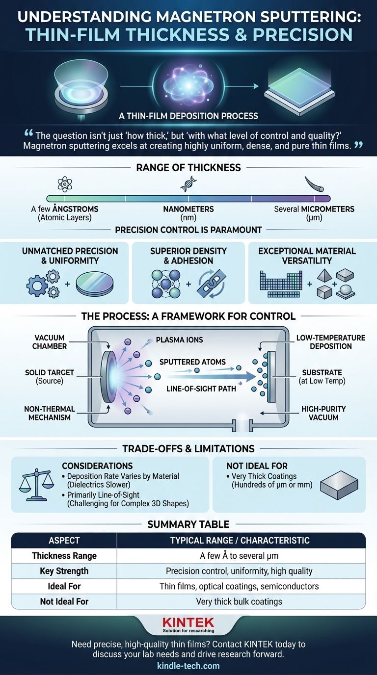
At its core, magnetron sputtering is a thin-film deposition process. The thickness of a film created by magnetron sputtering is not a single value but a highly controllable range. These films typically vary from a few angstroms (the thickness of single atoms) up to several micrometers (microns). The true strength of the process lies in its ability to precisely and uniformly deposit films within this range, not in creating thick, bulk layers.
The question isn't just "how thick," but "with what level of control and quality?" Magnetron sputtering excels at creating highly uniform, dense, and pure thin films, typically from nanometers to a few micrometers, where precision control over material properties is the primary goal.
The Defining Characteristics of Sputtered Films
To understand the role of thickness, you must first understand the fundamental qualities that magnetron sputtering imparts to a material. The thickness is simply one parameter within a system defined by precision and quality.
Unmatched Precision and Uniformity
The process allows for atomic-level control over film growth. This results in coatings that are exceptionally uniform across a surface.
This uniformity can be maintained even on large-area substrates, making it a reliable choice for industrial-scale production of sensitive components like semiconductor wafers or architectural glass.
Superior Film Density and Adhesion
During sputtering, high-energy atoms are ejected from a source material (the "target") and bombard the substrate. These energetic particles can penetrate the substrate surface slightly.
This creates an exceptionally strong bond between the film and the substrate, resulting in films with extremely high adhesion. The resulting film is also very dense and free of voids, which enhances its protective qualities and performance.
Exceptional Material Versatility
Magnetron sputtering is remarkably flexible. It can be used to deposit almost any metal, alloy, or compound, including high-melting-point materials that are impossible to deposit using thermal evaporation.
By using multiple targets (co-sputtering) or introducing reactive gases like nitrogen or oxygen into the vacuum chamber, complex alloys and ceramic compounds (like nitrides and oxides) can be created with precise stoichiometry.
The Sputtering Process: A Framework for Control
The advantages of sputtered films are a direct result of the process itself. Understanding how it works reveals why it is the superior choice for specific applications.
From Solid Target to Plasma
Unlike methods that melt material, sputtering uses a plasma in a vacuum to bombard a solid target with ions. This knocks atoms off the target, which then travel and deposit onto the substrate.
This physical, non-thermal mechanism is what enables the deposition of complex alloys and high-temperature materials without altering their composition.
Low-Temperature Deposition
The substrate can remain at or near room temperature during deposition. The energy is in the sputtered particles, not in the bulk environment.
This makes magnetron sputtering ideal for coating heat-sensitive substrates, such as plastics, flexible electronics, or already-processed semiconductor devices that would be damaged by high temperatures.
A High-Purity Vacuum Environment
The entire process is conducted under a high vacuum, which removes atmospheric gases and other impurities.
This ensures the resulting film is of high purity, as there is minimal risk of contamination being incorporated into the coating during its growth.
Understanding the Trade-offs and Limitations
No technology is without its compromises. A clear-eyed view of sputtering's limitations is critical for making an informed decision.
Deposition Rate Varies by Material
While sputtering is praised for high deposition rates, this is highly dependent on the material. Metals generally sputter very quickly.
However, dielectric materials like ceramics and oxides can have significantly lower deposition rates, which can impact production time and cost for certain applications.
Primarily a Line-of-Sight Process
Sputtered atoms travel in a relatively straight line from the target to the substrate. While particle scattering provides some coverage on the sides of features, it is fundamentally a line-of-sight process.
Coating highly complex 3D shapes or the inside of deep, narrow trenches can be challenging and may require sophisticated substrate rotation and manipulation to achieve uniformity.
High Initial Equipment Cost
The complexity of vacuum chambers, high-voltage power supplies, and magnetic assemblies means that sputtering systems represent a significant capital investment compared to simpler methods like electroplating or wet chemical deposition.
Not Ideal for Very Thick Coatings
The process is optimized for precision in the nanometer-to-micrometer range. If your application requires a coating thickness of hundreds of micrometers or millimeters, other processes like thermal spray or cladding are far more efficient and cost-effective.
Making the Right Choice for Your Application
The decision to use magnetron sputtering should be driven by your end goal. The required thickness is a consequence of the performance you need.
- If your primary focus is advanced optical coatings or semiconductors: The exceptional uniformity and atomic-level control over nanometer-scale layers make sputtering an ideal choice.
- If your primary focus is durable protective coatings on tools or medical implants: The high film density and excellent adhesion provide superior wear resistance and biocompatibility.
- If your primary focus is rapid, thick-layer bulk coating: You should evaluate other methods like thermal spray or plating, as sputtering is optimized for precision thin films.
- If your primary focus is coating heat-sensitive plastics or electronics: The low-temperature nature of the process is a significant advantage over high-temperature evaporative techniques.
Ultimately, magnetron sputtering offers unparalleled control over the structure and properties of materials at the nanoscale.
Summary Table:
| Aspect | Typical Range / Characteristic |
|---|---|
| Thickness Range | A few Ångstroms (atomic layers) to several micrometers (microns) |
| Key Strength | Precision control, uniformity, and high-quality film properties |
| Ideal For | Thin films where control over material properties is critical |
| Not Ideal For | Very thick coatings (hundreds of micrometers/millimeters) |
Need precise, high-quality thin films for your application?
KINTEK specializes in advanced lab equipment, including magnetron sputtering systems, to help you achieve unparalleled control over film thickness, uniformity, and material properties. Whether you're working on semiconductors, optical coatings, or protective layers, our expertise ensures your lab has the right tools for success.
Contact us today to discuss how our solutions can meet your specific laboratory needs and drive your research forward.
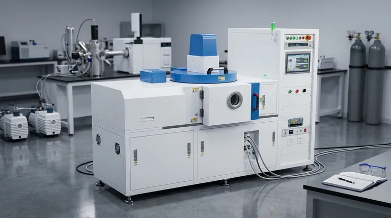
Visual Guide
Related Products
- Spark Plasma Sintering Furnace SPS Furnace
- RF PECVD System Radio Frequency Plasma-Enhanced Chemical Vapor Deposition RF PECVD
People Also Ask
- What is the theory of spark plasma sintering? A Guide to Rapid, Low-Temperature Densification
- What is the pressure for spark plasma sintering? A Guide to Optimizing SPS Parameters
- Why are Spark Plasma Sintering (SPS) furnaces or hot presses utilized in the preparation of Li3PS4 solid electrolytes?
- What are the fundamentals of spark plasma sintering process? Unlock Rapid, High-Performance Material Consolidation
- What is SPS sintering method? A Guide to High-Speed, High-Performance Material Fabrication

