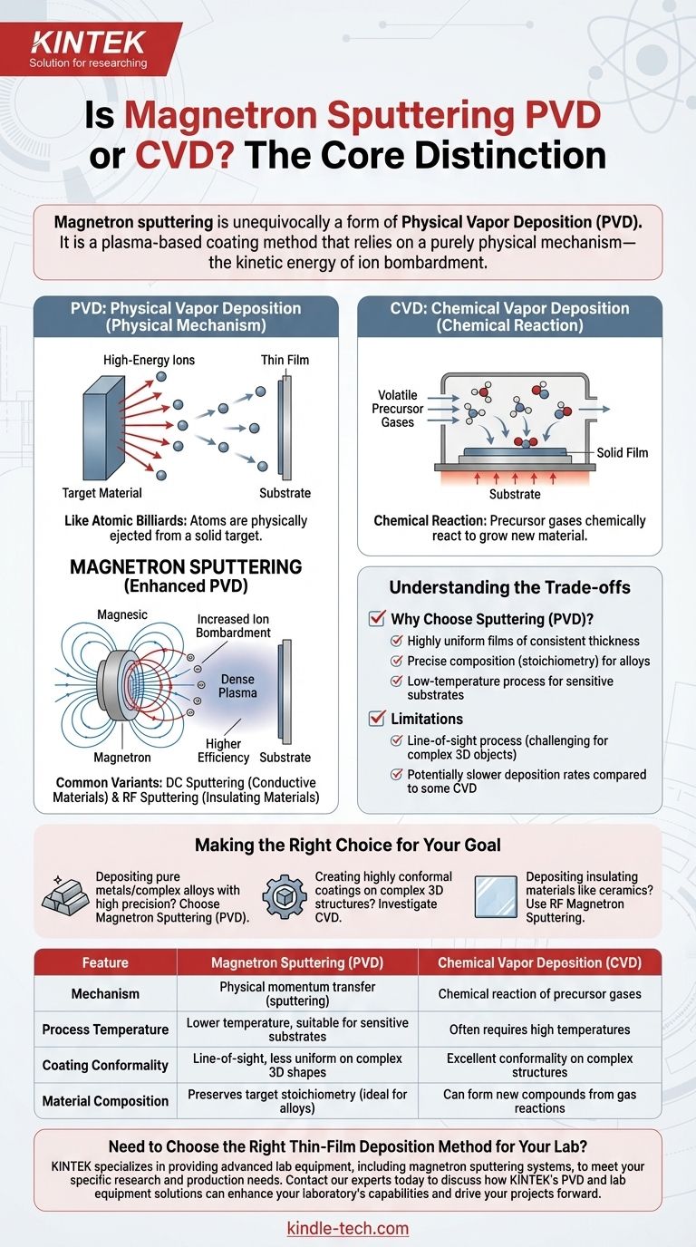
Magnetron sputtering is unequivocally a form of Physical Vapor Deposition (PVD). It is a plasma-based coating method that relies on a purely physical mechanism—the kinetic energy of ion bombardment—to transfer material from a source target to a substrate. This places it distinctly in the PVD category, separate from Chemical Vapor Deposition (CVD), which uses chemical reactions to form films.
The core distinction is simple: PVD physically moves atoms from a solid target to a substrate, like a microscopic spray paint. CVD uses precursor gases that chemically react at the substrate's surface to grow a new material. Magnetron sputtering is an advanced form of this physical "spraying" process.
The Core Distinction: Physical vs. Chemical Deposition
To understand why magnetron sputtering is PVD, it's essential to grasp the fundamental difference between these two major families of thin-film deposition.
Understanding Physical Vapor Deposition (PVD)
PVD encompasses a set of vacuum deposition methods where a material is transformed into a vapor phase through physical means.
The process is mechanical at an atomic level. A solid source material, known as the "target," is bombarded with energy, causing atoms or molecules to be ejected. These ejected particles then travel through a vacuum and condense onto a substrate, forming a thin film.
The Principle of Sputtering
Sputtering is a cornerstone PVD technique that functions like a game of atomic billiards.
High-energy ions, typically from an inert gas like argon, are accelerated toward the target material. The impact of these ions physically knocks atoms loose from the target's surface. This process is a non-thermal vaporization, driven entirely by momentum transfer.
What Defines Chemical Vapor Deposition (CVD)?
CVD operates on a completely different principle. It involves introducing one or more volatile precursor gases into a reaction chamber.
These gases decompose or react with each other on and near the heated substrate's surface, leaving behind a solid film. The defining characteristic is the chemical change from gas to solid, which is fundamentally absent in PVD sputtering.
How Magnetron Sputtering Refines the PVD Process
Magnetron sputtering is not a different category; it is a highly efficient and widely used evolution of the basic sputtering technique.
The Role of Plasma
Like other sputtering methods, the process begins by creating a plasma—a superheated, ionized gas—to serve as the source of high-energy ions for bombardment.
The "Magnetron" Enhancement
The key innovation is the use of a powerful magnetic field (from a magnetron) positioned behind the sputtering target.
This magnetic field traps electrons close to the target's surface. These trapped electrons are forced to travel in a spiral path, dramatically increasing the probability that they will collide with and ionize the neutral gas atoms.
This creates a much denser, more stable plasma directly in front of the target, leading to a significantly higher rate of ion bombardment and, consequently, a faster and more efficient deposition process.
Common Variants: DC vs. RF Sputtering
The technology is versatile, with two main types:
- DC (Direct Current) Sputtering: Ideal for depositing electrically conductive materials.
- RF (Radio Frequency) Sputtering: Used for depositing electrically insulating (dielectric) materials, as the alternating field prevents charge buildup on the target.
Understanding the Trade-offs
Choosing a deposition method requires understanding its inherent strengths and weaknesses.
Why Choose Sputtering (PVD)?
Magnetron sputtering is valued for its ability to produce highly uniform films of consistent thickness. Because it physically transfers the target material, it excels at depositing complex materials like alloys while precisely maintaining their original chemical composition (stoichiometry).
It is also a relatively low-temperature process compared to many CVD techniques, making it suitable for temperature-sensitive substrates.
Limitations and Considerations
Sputtering is a line-of-sight process. This means it can be challenging to achieve a uniform coating on complex, three-dimensional objects with deep trenches or hidden surfaces.
Furthermore, deposition rates for sputtering, while enhanced by the magnetron, can still be slower than some high-speed CVD or other PVD evaporation processes.
Making the Right Choice for Your Goal
Selecting the correct method depends entirely on the material you are depositing and the desired properties of the final film.
- If your primary focus is depositing pure metals or complex alloys with high precision: Magnetron sputtering is an excellent choice due to its physical transfer mechanism that preserves material composition.
- If your primary focus is creating highly conformal coatings on complex 3D structures: You should investigate CVD, as its gas-phase chemical reaction process is not limited by line-of-sight deposition.
- If your primary focus is depositing insulating materials like ceramics or oxides: RF Magnetron Sputtering is the specific PVD technique designed to handle these non-conductive targets effectively.
Understanding the fundamental distinction between physical and chemical processes is the key to selecting the ideal thin-film deposition technology for your application.
Summary Table:
| Feature | Magnetron Sputtering (PVD) | Chemical Vapor Deposition (CVD) |
|---|---|---|
| Mechanism | Physical momentum transfer (sputtering) | Chemical reaction of precursor gases |
| Process Temperature | Lower temperature, suitable for sensitive substrates | Often requires high temperatures |
| Coating Conformality | Line-of-sight, less uniform on complex 3D shapes | Excellent conformality on complex structures |
| Material Composition | Preserves target stoichiometry (ideal for alloys) | Can form new compounds from gas reactions |
Need to Choose the Right Thin-Film Deposition Method for Your Lab?
Understanding the difference between PVD and CVD is critical for achieving your desired coating results. KINTEK specializes in providing advanced lab equipment, including magnetron sputtering systems, to meet your specific research and production needs.
Whether you're depositing pure metals, complex alloys, or insulating ceramics, our expertise ensures you get the right solution for precise, high-quality thin films.
Contact our experts today to discuss how KINTEK's PVD and lab equipment solutions can enhance your laboratory's capabilities and drive your projects forward.
Visual Guide
Related Products
- RF PECVD System Radio Frequency Plasma-Enhanced Chemical Vapor Deposition RF PECVD
- Inclined Rotary Plasma Enhanced Chemical Vapor Deposition PECVD Equipment Tube Furnace Machine
- 915MHz MPCVD Diamond Machine Microwave Plasma Chemical Vapor Deposition System Reactor
- HFCVD Machine System Equipment for Drawing Die Nano-Diamond Coating
- Vacuum Hot Press Furnace Machine for Lamination and Heating
People Also Ask
- Why does PECVD commonly use RF power input? For Precise Low-Temperature Thin Film Deposition
- What is the principle of plasma enhanced chemical vapor deposition? Achieve Low-Temperature Thin Film Deposition
- Why is PECVD environment friendly? Understanding the Eco-Friendly Benefits of Plasma-Enhanced Coating
- What is an example of PECVD? RF-PECVD for High-Quality Thin Film Deposition
- What are the applications of PECVD? Essential for Semiconductors, MEMS, and Solar Cells