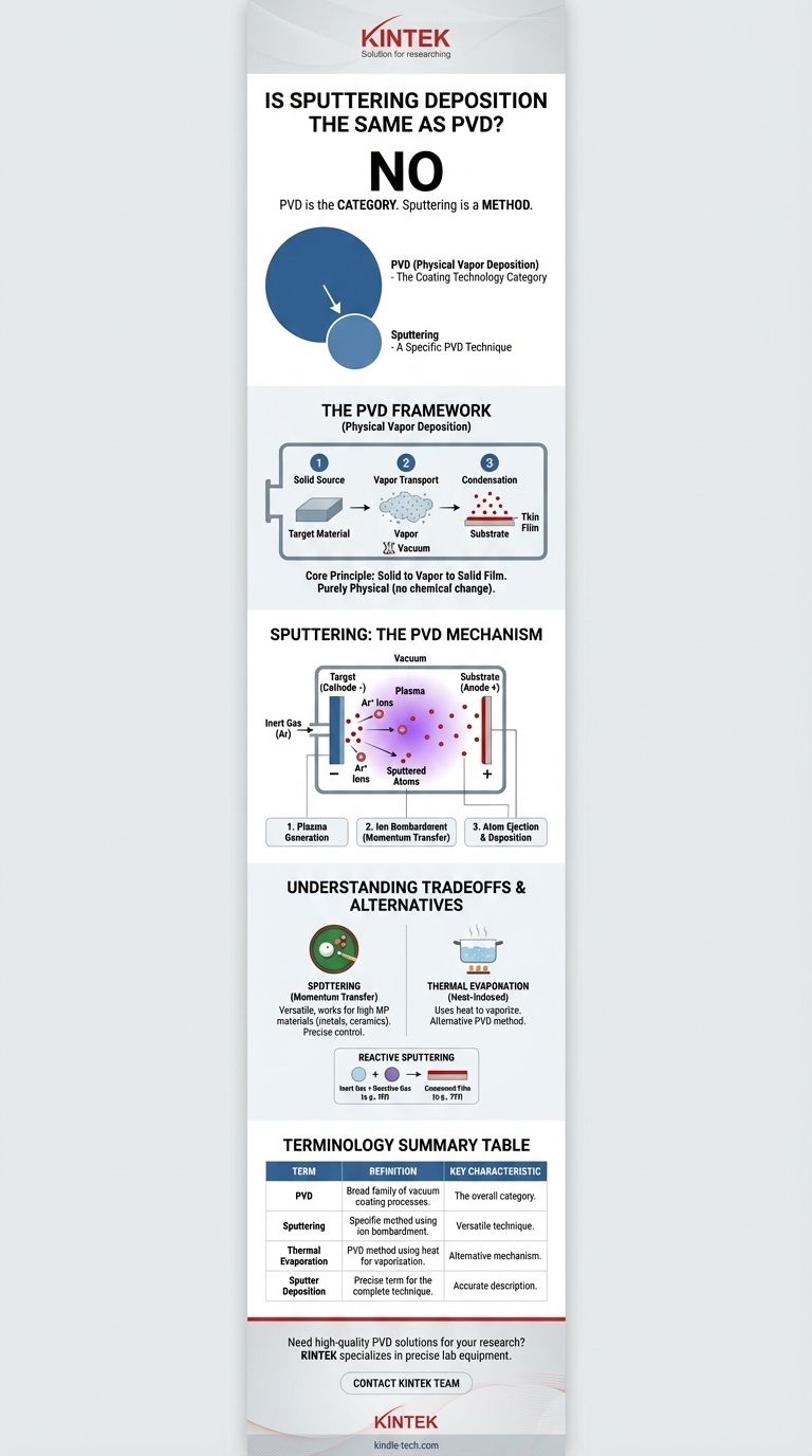
No, sputtering is not the same as Physical Vapor Deposition (PVD). Rather, sputtering is one of the primary methods used to carry out a PVD process. Think of PVD as the overall category of a coating technology, while sputtering is a specific technique within that category.
The core distinction is simple: Physical Vapor Deposition (PVD) is the broad name for a class of vacuum deposition processes, whereas sputtering is a specific mechanism—using ion bombardment to create a vapor—to achieve PVD.
What is Physical Vapor Deposition (PVD)?
The Core Principle of PVD
Physical Vapor Deposition is a family of processes used to create very thin films of material on a surface, known as a substrate. All PVD processes share a fundamental, three-step sequence that occurs within a vacuum chamber.
First, a solid source material (the "target") is converted into a vapor. Second, this vapor is transported through the vacuum. Third, the vapor condenses onto the substrate, forming a thin, solid film.
The "Physical" Distinction
The term "physical" is key. In its purest form, PVD moves atoms from a source to a substrate without inducing a chemical reaction. The material of the coating is the same as the material of the source target.
How Sputtering Fits into the PVD Framework
Sputtering as a PVD Mechanism
Sputtering is the answer to the first step of the PVD sequence: how do you turn the solid source material into a vapor? It is one of the most common and versatile methods to achieve this.
The Mechanics of Sputtering
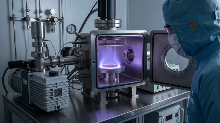
The process begins by introducing an inert gas, typically argon, into the vacuum chamber and generating a plasma. This plasma creates a sea of high-energy, positively charged argon ions.
A high voltage is applied to the target material, causing these ions to accelerate and collide with it at great force. This energetic bombardment is like a microscopic game of billiards, where the argon ions are the cue balls.
The Deposition of Sputtered Atoms
When the ions strike the target, their kinetic energy physically dislodges, or "sputters," individual atoms from the source material. These ejected atoms then travel across the chamber and deposit uniformly onto the substrate, creating the desired thin film.
Understanding the Trade-offs and Alternatives
The Sputtering Advantage
Sputtering is an extremely versatile PVD technique. Because it relies on momentum transfer rather than heat, it can be used to deposit a vast range of materials, including metals, alloys, and ceramics with very high melting points that are difficult to vaporize by other means.
Contrast with Thermal Evaporation
To fully understand the distinction, consider another major PVD method: thermal evaporation. In this process, the source material is heated in the vacuum until it boils and evaporates, creating a vapor that then condenses on the substrate.
Both sputtering and thermal evaporation are PVD processes. The end goal is the same, but the mechanism for creating the vapor—ion bombardment versus heat—is fundamentally different.
The Flexibility of Reactive Sputtering
Sputtering can also be adapted to intentionally create a chemical reaction. By introducing a reactive gas (like nitrogen or oxygen) along with the inert gas, new compounds can be formed. For example, sputtering a titanium target in the presence of nitrogen gas will create an extremely hard coating of titanium nitride (TiN) on the substrate.
Making the Right Choice in Terminology
To communicate clearly, it's essential to use these terms correctly. Your choice depends on the level of detail you need to convey.
- If your primary focus is the general class of vacuum coating processes: Use the term Physical Vapor Deposition (PVD).
- If your primary focus is the specific method of using ion bombardment to eject atoms: Use the term sputtering.
- If your primary focus is describing the complete technique with precision: Use sputter deposition or PVD by sputtering.
Understanding this distinction allows you to accurately describe and evaluate coating technologies for any application.
Summary Table:
| Term | Definition | Key Characteristic |
|---|---|---|
| Physical Vapor Deposition (PVD) | A family of vacuum processes for depositing thin films. | The broad category; includes sputtering and evaporation. |
| Sputtering | A specific PVD method that uses ion bombardment to eject atoms from a target. | A versatile technique within the PVD framework. |
| Thermal Evaporation | Another PVD method that uses heat to vaporize the source material. | An alternative to sputtering for creating the vapor. |
Need a high-quality, uniform thin film for your research or production? The right PVD technique is critical for your project's success. KINTEK specializes in lab equipment and consumables, providing the precise sputtering and PVD solutions that laboratories rely on for cutting-edge materials science. Let our experts help you select the ideal system for your specific application. Contact our team today to discuss your coating requirements!
Visual Guide
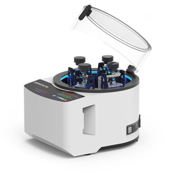
Related Products
- Inclined Rotary Plasma Enhanced Chemical Vapor Deposition PECVD Equipment Tube Furnace Machine
- Lab Plastic PVC Calender Stretch Film Casting Machine for Film Testing
- Vacuum Hot Press Furnace Machine for Lamination and Heating
- HFCVD Machine System Equipment for Drawing Die Nano-Diamond Coating
- 915MHz MPCVD Diamond Machine Microwave Plasma Chemical Vapor Deposition System Reactor
People Also Ask
- How many types of sputtering are there? A Guide to DC, RF, and Advanced Techniques
- How many types of vapor phase deposition techniques are present? PVD vs. CVD Explained
- What is a sputtering system? Achieve Unmatched Thin Film Deposition for Your Lab
- Is sputtering a PVD? Discover the Key Coating Technology for Your Lab
- How does a sputtering machine work? Achieve Atomic-Level Precision for Your Coatings