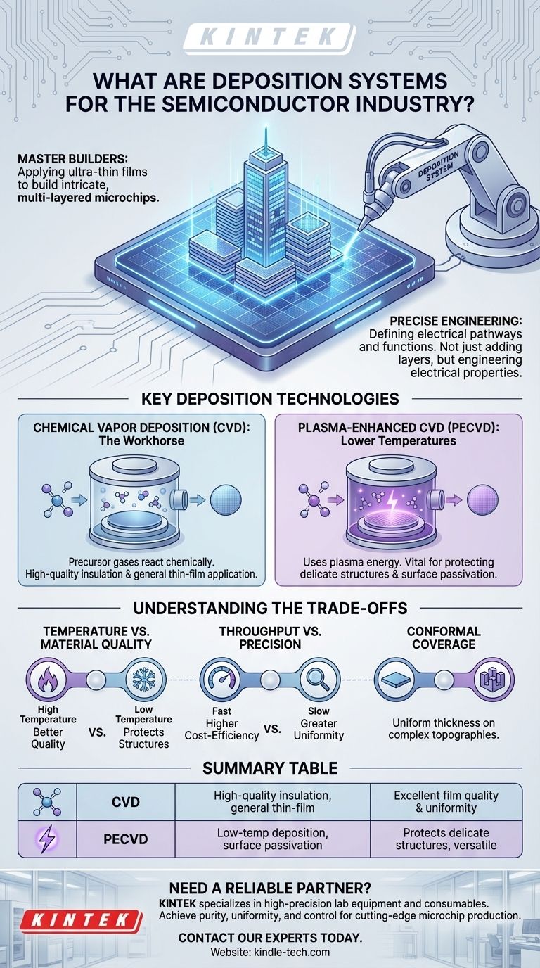
In semiconductor manufacturing, deposition systems are the master builders. These are highly specialized machines that apply ultra-thin layers of material, known as thin films, onto a silicon wafer. This process meticulously builds the intricate, multi-layered structures that form modern microchips, with technologies like Chemical Vapor Deposition (CVD) serving as a cornerstone of the industry.
At its core, deposition is not just about adding a layer; it's about precisely engineering the electrical properties of a chip. The choice of deposition system and method directly determines the performance, reliability, and function of the final semiconductor device.
The Fundamental Role of Deposition
Building a Chip, Layer by Layer
Think of a microchip as a microscopic, multi-story skyscraper. Deposition systems are the equipment used to construct each floor.
Each "floor" is a film of material, often thousands of times thinner than a human hair, that performs a specific function within the chip's integrated circuit.
Defining Electrical Pathways and Functions
These layers are not random. Deposition systems are used to apply both insulating (dielectric) and conducting (metallic) materials with extreme precision.
By depositing these materials in specific patterns, engineers create the wires, transistors, and insulators that form the complex electrical circuits of a processor or memory chip. Applications mentioned in the references, such as the "isolation of conductive layers," are a perfect example of this.
The Importance of Purity and Control
The performance of a semiconductor device is critically dependent on the quality of these deposited films. The layers must be incredibly uniform, pure, and free of defects.
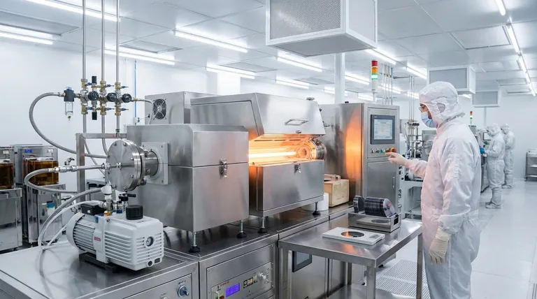
This is why deposition occurs inside highly controlled reaction chambers within pristine clean rooms. The entire environment, including the air itself, is filtered and managed to prevent contaminants from ruining the microscopic circuitry.
Key Deposition Technologies
Chemical Vapor Deposition (CVD): The Workhorse
CVD is the most common deposition technology. It works by introducing one or more precursor gases into a reaction chamber containing the silicon wafers.
These gases undergo a chemical reaction, causing a new, solid material to form and deposit itself as a thin film evenly across the wafer surfaces. It's used for a wide variety of insulating and metallic materials.
Plasma-Enhanced CVD (PECVD): Lower Temperatures, More Flexibility
PECVD is a crucial variant of CVD. It uses an energy source, plasma, to stimulate the chemical reaction.
The key benefit is that this allows deposition to occur at much lower temperatures. This is vital for protecting delicate structures that have already been built on the wafer in previous steps. PECVD is commonly used for final protective layers (surface passivation) and device encapsulation.
Understanding the Trade-offs
Temperature vs. Material Quality
The "thermal budget" is a critical constraint in chip manufacturing. High-temperature deposition processes can produce very high-quality films, but they can also damage or alter previously deposited layers.
Choosing a deposition method often involves balancing the need for a high-quality film against the temperature sensitivity of the existing device structure. This is why lower-temperature methods like PECVD are essential.
Throughput vs. Precision
The speed at which a system can process wafers (throughput) directly impacts the cost of manufacturing. However, faster deposition processes can sometimes compromise the uniformity or structural quality of the film.
Engineers must constantly optimize this trade-off, selecting a process that is fast enough to be economical but precise enough to meet the device's strict performance requirements.
Conformal Coverage on Complex Structures
Modern chips have incredibly complex 3D topographies. A major challenge for deposition systems is ensuring the deposited film covers these vertical and horizontal surfaces with a perfectly uniform thickness.
Some deposition techniques are superior at this "conformal coverage" than others, and the choice depends heavily on the specific structure being built.
Making the Right Choice for Your Goal
The right deposition system is determined entirely by the specific function of the layer being created.
- If your primary focus is creating high-quality insulation between components: CVD and PECVD are the industry standard for depositing materials like silicon dioxide and silicon nitride.
- If your primary focus is protecting the final device from the environment: PECVD is the preferred method for applying final passivation and encapsulation layers due to its lower processing temperatures.
- If your primary focus is creating an anti-reflective coating for optical sensors: Specific CVD processes are tuned to deposit layers with precise optical properties for this purpose.
Ultimately, deposition systems are the foundational tools that translate an abstract circuit design into a physical, functioning microchip.
Summary Table:
| Key Deposition Technology | Primary Function | Key Advantage |
|---|---|---|
| Chemical Vapor Deposition (CVD) | High-quality insulation, general thin-film application | Excellent film quality and uniformity |
| Plasma-Enhanced CVD (PECVD) | Low-temperature deposition, surface passivation | Protects delicate structures, versatile |
Need a reliable partner for your semiconductor deposition needs? KINTEK specializes in high-precision lab equipment and consumables for the semiconductor industry. Our expertise in deposition technologies can help you achieve the purity, uniformity, and control required for cutting-edge microchip production. Contact our experts today to discuss how our solutions can enhance your semiconductor manufacturing process.
Visual Guide
Related Products
- Chemical Vapor Deposition CVD Equipment System Chamber Slide PECVD Tube Furnace with Liquid Gasifier PECVD Machine
- 915MHz MPCVD Diamond Machine Microwave Plasma Chemical Vapor Deposition System Reactor
- Customer Made Versatile CVD Tube Furnace Chemical Vapor Deposition Chamber System Equipment
- HFCVD Machine System Equipment for Drawing Die Nano-Diamond Coating
- Split Chamber CVD Tube Furnace with Vacuum Station Chemical Vapor Deposition System Equipment Machine
People Also Ask
- What are the core advantages of PE-CVD in OLED encapsulation? Protect Sensitive Layers with Low-Temp Film Deposition
- What is plasma enhanced chemical vapor deposition PECVD equipment? A Guide to Low-Temperature Thin Film Deposition
- What happens during deposition chemistry? Building Thin Films from Gaseous Precursors
- What are the advantages of chemical vapor deposition? Achieve Superior Thin Films for Your Lab
- Why is Chemical Vapor Deposition (CVD) equipment uniquely suited for constructing hierarchical superhydrophobic structures?


