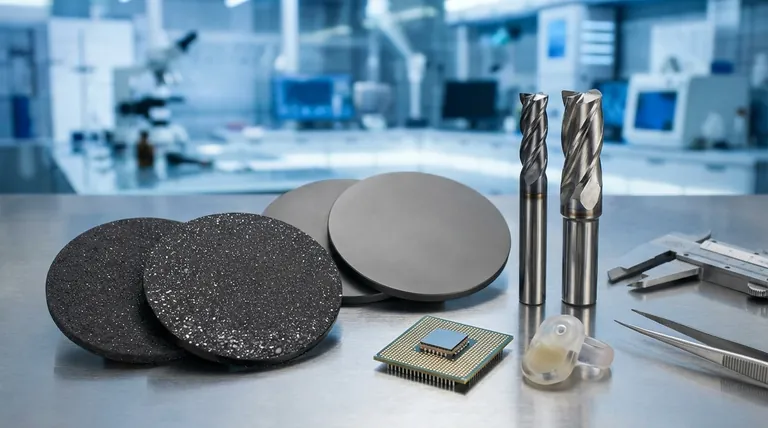
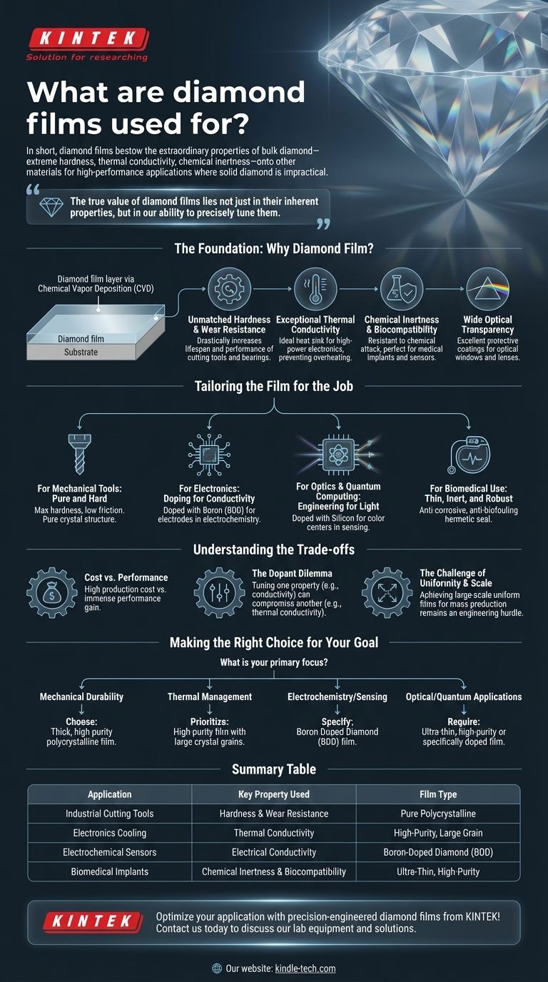
In short, diamond films are used to bestow the extraordinary properties of bulk diamond—like extreme hardness, thermal conductivity, and chemical inertness—onto the surface of other materials. This enables high-performance applications in industrial cutting tools, electronics cooling, electrochemistry, and biomedical implants where using solid diamond would be impractical or prohibitively expensive.
The true value of diamond films lies not just in their inherent properties, but in our ability to precisely tune them. By controlling the growth process and introducing specific dopants, we can engineer a film optimized for a specific task, whether it's conducting electricity, managing heat, or interacting with light.
The Foundation: Why Diamond Film?
At its core, the use of diamond film is about leveraging a unique combination of extreme material properties. These films are typically grown using Chemical Vapor Deposition (CVD), which allows a thin layer of diamond to be synthesized on a substrate.
Unmatched Hardness and Wear Resistance
Diamond is the hardest known natural material. Applying a diamond film to cutting tools, bearings, or valve rings drastically increases their lifespan and performance by protecting them from abrasion and wear.
Exceptional Thermal Conductivity
Diamond conducts heat better than any other material, including copper. This makes it an ideal heat sink for dissipating the intense heat generated by high-power electronics, lasers, and transistors, preventing them from overheating and failing.
Chemical Inertness and Biocompatibility
Diamond is extremely resistant to chemical attack and corrosion. This stability, combined with its biocompatibility, makes it perfect for coating medical implants or creating robust electrochemical sensors that can operate in harsh environments.
Wide Optical Transparency
High-quality diamond is transparent across a broad spectrum of light, from ultraviolet (UV) to far-infrared (IR). This makes thin diamond films excellent protective coatings for optical windows and lenses used in demanding environments.
Tailoring the Film for the Job
A diamond film is not a one-size-fits-all solution. Its properties are intentionally modified during manufacturing to meet the demands of a specific application. This is often achieved by introducing impurities, or dopants, into the diamond's crystal structure.
For Mechanical Tools: Pure and Hard
For applications like cutting tools, the goal is maximum hardness and a low coefficient of friction. These films are typically grown to be as pure as possible to maintain the ideal diamond crystal structure.
For Electronics: Doping for Conductivity
Pure diamond is an excellent electrical insulator. However, by doping it with boron, it becomes a semiconductor known as Boron-Doped Diamond (BDD). BDD is widely used to create highly durable and efficient electrodes for electrochemistry and water treatment.
For Optics and Quantum Computing: Engineering for Light
For advanced optical applications, specific "color centers" can be created within the diamond. Doping with silicon, for example, creates Silicon-Vacancy (SiV) centers that have unique quantum-optical properties, making them useful in sensing and quantum information processing.
For Biomedical Use: Thin, Inert, and Robust
In biomedical devices, ultra-thin diamond films provide a powerful combination of benefits. They act as a hermetic seal that is anti-corrosive and anti-biofouling (resists protein attachment), while also being mechanically robust and transparent for any embedded optical sensors.
Understanding the Trade-offs
While its properties are exceptional, deploying diamond film involves critical engineering and economic trade-offs.
Cost vs. Performance
Growing high-quality diamond film is a complex and energy-intensive process. The primary trade-off is balancing the immense performance gain against the manufacturing cost, especially when coating large or complex-shaped objects.
The Dopant Dilemma: Optimizing One Property at a Time
Tuning a film for one property can compromise another. For example, doping diamond with boron to increase electrical conductivity will simultaneously alter its optical properties and may slightly reduce its thermal conductivity. The film must be engineered for its primary function.
The Challenge of Uniformity and Scale
Achieving a perfectly uniform, high-quality film over a large surface area remains an engineering challenge. Scaling up production to reduce costs is a constant focus of research and development, as it is the key to unlocking new applications like non-stick cookware coatings.
Making the Right Choice for Your Goal
Selecting the right type of diamond film depends entirely on the problem you are trying to solve. Your decision should be guided by the primary performance driver required.
- If your primary focus is mechanical durability: Choose a thick, high-purity polycrystalline diamond film to maximize hardness and wear resistance.
- If your primary focus is thermal management: Prioritize a high-purity film with large crystal grains to ensure the highest possible thermal conductivity.
- If your primary focus is electrochemistry or sensing: Specify a Boron-Doped Diamond (BDD) film with a controlled level of doping to achieve the desired conductivity.
- If your primary focus is optical or quantum applications: Require an ultra-thin, high-purity film for transparency or a specifically doped film (e.g., silicon) to create active color centers.
By understanding how to tune diamond's fundamental properties, you can deploy it as a powerful solution for the most demanding engineering challenges.
Summary Table:
| Application | Key Property Used | Film Type |
|---|---|---|
| Industrial Cutting Tools | Hardness & Wear Resistance | Pure Polycrystalline |
| Electronics Cooling | Thermal Conductivity | High-Purity, Large Grain |
| Electrochemical Sensors | Electrical Conductivity | Boron-Doped Diamond (BDD) |
| Biomedical Implants | Chemical Inertness & Biocompatibility | Ultra-Thin, High-Purity |
Optimize your application with precision-engineered diamond films from KINTEK! Whether you need enhanced durability for cutting tools, superior thermal management for electronics, or reliable coatings for medical devices, our lab equipment and consumables are tailored to meet your specific requirements. Contact us today to discuss how our diamond film solutions can bring unmatched performance and longevity to your laboratory or production line.
Visual Guide
Related Products
- Custom CVD Diamond Coating for Lab Applications
- Laboratory CVD Boron Doped Diamond Materials
- CVD Diamond Optical Windows for Lab Applications
- CVD Diamond Domes for Industrial and Scientific Applications
- CVD Diamond Wire Drawing Die Blanks for Precision Applications
People Also Ask
- What is CVD diamond coating? Grow a Super-Hard, High-Performance Diamond Layer
- What are the types of CVD coating? A Guide to Choosing the Right Process
- What are the advantages of CVD coating? Superior Hardness and Uniformity for Demanding Applications
- Can you coat something in diamond? Unlock Unmatched Hardness and Thermal Conductivity
- What is CVD coating? Transform Your Material's Surface for Maximum Performance


