At its core, Metalorganic Chemical Vapor Deposition (MOCVD) is a dominant technology for manufacturing high-performance compound semiconductor devices like LEDs and lasers. Its primary advantage is the ability to grow high-quality, complex crystalline layers at a scale suitable for mass production. However, this capability is fundamentally tied to its main disadvantage: the use of highly toxic and pyrophoric precursor materials, which introduces significant safety, facility, and cost challenges.
The decision to use MOCVD is a strategic trade-off. You are choosing a process that offers unparalleled scalability and control over material composition, but you must be prepared to manage the inherent complexities and safety risks of its chemical precursors.
The Core Advantages of MOCVD
MOCVD (also known as OMVPE) became the industrial standard for specific applications because its advantages directly enable the mass production of complex electronic and optoelectronic devices.
High-Volume Scalability
The most significant advantage of MOCVD is its throughput. The process operates at moderate pressures, allowing for reactor designs that can hold multiple wafers (multi-wafer systems) in a single run.
This is the primary reason MOCVD dominates the manufacturing of LEDs, where cost-per-unit is a critical driver. It effectively bridges the gap between laboratory-scale crystal growth and industrial-scale production.
Exceptional Crystal Quality
MOCVD is a form of epitaxial growth, meaning the deposited atoms arrange themselves into a high-quality, single-crystal film that follows the crystal structure of the underlying substrate.
This results in materials with very low defect densities, which is essential for the efficiency and reliability of devices like high-brightness LEDs, laser diodes, and high-frequency transistors.
Precise Control Over Heterostructures
Modern semiconductor devices are rarely made of a single material. They are heterostructures, built from many thin layers of different materials or alloys.
MOCVD provides excellent and rapid control over film composition and thickness. By simply adjusting the gas flows into the reactor, engineers can create atomically sharp interfaces between layers, which is crucial for creating quantum wells and other complex device structures.
Versatile Doping and Alloying
Introducing impurities to control electrical properties (doping) or mixing elements to create alloys (e.g., AlxGa1-xAs) is straightforward in MOCVD.
Dopant and alloy precursors are introduced as gases, and their concentrations can be precisely managed by mass flow controllers. This allows for fine-tuning of a material's electronic and optical properties during the growth process itself.
The Critical Disadvantages and Challenges
The power of MOCVD comes at a price. The challenges are not minor considerations; they are core aspects of the technology that dictate facility design, operational protocols, and overall cost.
Extreme Safety Hazards
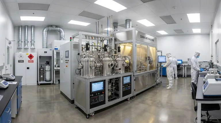
MOCVD relies on metalorganic precursors (like trimethylgallium) and hydride gases (like arsine and phosphine). Many of these materials are highly toxic and pyrophoric, meaning they can spontaneously ignite on contact with air.
This necessitates an extensive and costly safety infrastructure, including dedicated gas cabinets, redundant leak detectors, emergency ventilation, and abatement systems (scrubbers) to treat the exhaust gas. Operator training and safety protocols are paramount.
High Operational and Capital Costs
The specialized equipment required to handle hazardous gases safely makes MOCVD reactors expensive. The high-purity precursor chemicals themselves are also a significant recurring operational cost.
Furthermore, the process consumes large amounts of carrier gases like hydrogen and nitrogen, adding to the overall expense.
Complex Reaction Chemistry
Unlike a purely physical deposition process like Molecular Beam Epitaxy (MBE), MOCVD is a chemical one. The precursor gases must decompose at high temperatures and react on the wafer surface, creating complex chemical byproducts.
This complexity can lead to unintentional incorporation of impurities, particularly carbon from the metalorganic molecules. Managing these reactions to achieve the desired film purity and uniformity can be a significant engineering challenge.
High Process Temperatures
MOCVD typically operates at very high temperatures (500-1100°C) to facilitate the chemical reactions needed for high-quality film growth.
These high temperatures can limit the types of substrates that can be used. It can also cause unwanted effects in the device structure, such as the diffusion of dopants from one layer into another, potentially degrading device performance.
Understanding the Trade-offs: MOCVD vs. MBE
To fully grasp the context of MOCVD's pros and cons, it is useful to compare it to its main alternative for high-quality epitaxial growth: Molecular Beam Epitaxy (MBE).
Growth Rate vs. Purity
MOCVD offers significantly higher growth rates, making it ideal for thick layers and production environments.
MBE is a slower, ultra-high vacuum technique that offers unparalleled purity and precision, often achieving monolayer control. It is frequently the choice for cutting-edge research and devices where ultimate material purity is the top priority.
Scalability and Cost
MOCVD is designed for scalability. Multi-wafer systems are the industry standard for LED production.
MBE systems are typically single-wafer and have lower throughput, making them less cost-effective for high-volume manufacturing but perfectly suited for research and development.
Making the Right Choice for Your Goal
Choosing MOCVD is not just a technical choice; it's a strategic one based on your final objective.
- If your primary focus is mass production of established devices (e.g., GaN LEDs): MOCVD is the undisputed choice due to its high throughput and proven scalability.
- If your primary focus is fundamental research or creating novel devices with the absolute highest purity: MBE is often the superior option, offering more precise control in a cleaner environment.
- If your primary focus is developing new compound semiconductor devices for future production: The choice is more nuanced, but MOCVD is often favored if a clear path to scalable manufacturing is a key requirement.
Ultimately, selecting MOCVD is a deliberate decision to embrace its chemical and operational complexity in exchange for unparalleled manufacturing scale.
Summary Table:
| Aspect | Advantage | Disadvantage |
|---|---|---|
| Production | High-volume scalability for mass manufacturing | High capital and operational costs |
| Material Quality | Exceptional crystal quality & precise heterostructure control | Complex chemistry can lead to carbon impurities |
| Process | Versatile doping and alloying capabilities | Requires high temperatures, limiting substrate options |
| Safety & Handling | Industry-standard for devices like LEDs | Uses highly toxic, pyrophoric precursors requiring extensive safety measures |
Ready to scale your semiconductor or LED production with reliable lab equipment? KINTEK specializes in providing robust laboratory solutions, including support for advanced processes like MOCVD. Our expertise in lab equipment and consumables ensures you have the tools needed for efficient, high-quality material growth. Contact our experts today to discuss how we can support your specific laboratory needs and help you achieve your production goals.
Visual Guide

Related Products
- 915MHz MPCVD Diamond Machine Microwave Plasma Chemical Vapor Deposition System Reactor
- HFCVD Machine System Equipment for Drawing Die Nano-Diamond Coating
- Vacuum Hot Press Furnace Machine for Lamination and Heating
- Inclined Rotary Plasma Enhanced Chemical Vapor Deposition PECVD Equipment Tube Furnace Machine
- Vacuum Heat Treat and Molybdenum Wire Sintering Furnace for Vacuum Sintering
People Also Ask
- How does MPCVD work? A Guide to Low-Temperature, High-Quality Film Deposition
- What is the microwave plasma method? A Guide to High-Purity Material Synthesis
- What are the limitations of diamonds? Beyond the Myth of Perfection
- What is microwave plasma CVD? A Guide to High-Purity Diamond and Material Synthesis
- What are the primary advantages of the CVD method for growing diamonds? Engineering High-Purity Gems and Components
