The primary advantages of Chemical Vapor Deposition (CVD) are its exceptional versatility, its ability to produce highly pure and durable films, and its unique capacity to uniformly coat complex, non-flat surfaces. Because it relies on a chemical reaction from a vapor phase rather than a direct line-of-sight spray, CVD can create high-performance coatings in places that other methods simply cannot reach.
The true power of CVD is not just in creating high-quality thin films, but in its fundamental flexibility. It gives engineers precise control over material properties on a vast range of substrates and geometries, making it an essential tool for advanced manufacturing.
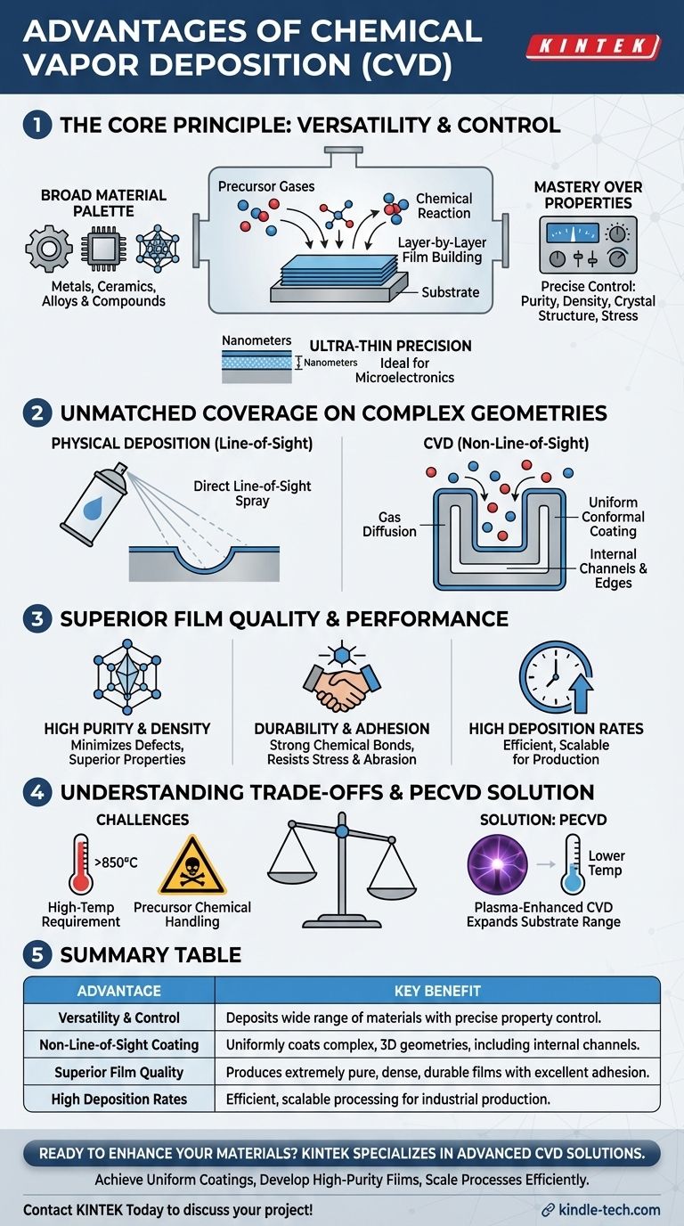
The Core Principle: Versatility and Control
The foundation of CVD's advantages lies in its process: precursor gases are introduced into a chamber where they react and decompose on a substrate's surface, building a solid film layer by layer. This chemical basis provides an unparalleled level of control.
A Broad Palette of Materials
CVD is not limited to a single type of material. Its chemical nature allows for the deposition of a wide array of substances, including metals, ceramics, multi-component alloys, and other compounds.
This makes it adaptable to countless applications, from creating corrosion-resistant metal coatings to producing high-purity ceramic layers for electronics.
Mastery Over Film Properties
By carefully adjusting deposition parameters like gas composition, flow rate, temperature, and pressure, you can precisely engineer the film's final characteristics.
This includes controlling the material's purity, density, crystal structure, grain size, and even its residual stress. This level of fine-tuning is critical for high-performance applications.
Ultra-Thin Layer Precision
The process allows for the creation of ultra-thin layers with exceptional uniformity. This makes CVD indispensable for the semiconductor industry in the production of electrical circuits and microelectronics, where layer thickness is measured in nanometers.
Unmatched Coverage on Complex Geometries
One of the most significant distinctions of CVD is its ability to coat surfaces that are not in a direct line of sight from the material source.
The "Non-Line-of-Sight" Advantage
Unlike physical deposition methods (like sputtering) which act like a spray paint can, the precursor gases in a CVD process flow and diffuse throughout the entire chamber.
These gases envelop the substrate, allowing the chemical reaction to occur on all exposed surfaces simultaneously, regardless of their orientation.
Uniform and Conformal Coatings
The result is an exceptionally uniform and conformal coating that perfectly follows the contours of even the most intricate and complex shapes. This "wrap-around" capability ensures that internal channels, sharp edges, and detailed features receive the same high-quality film as flat surfaces.
Superior Film Quality and Performance
The films produced by CVD are known for their high quality and robust performance characteristics, which stem directly from the controlled, bottom-up deposition process.
High Purity and Density
Because the process starts with high-purity precursor gases and a controlled reaction, the resulting films are themselves extremely pure and dense. This minimizes defects and voids, leading to superior material properties.
Durability and Adhesion
CVD coatings form strong chemical bonds with the substrate, resulting in excellent adhesion. These durable films can withstand high-stress environments, abrasion, and extreme temperature variations without delaminating.
High Deposition Rates
For many materials, CVD offers a comparatively high deposition rate and manufacturing yield. This efficiency, combined with the relative simplicity of the equipment, makes the process easy to scale for industrial production.
Understanding the Trade-offs
No process is without its limitations. Being an effective technical advisor means acknowledging the challenges associated with CVD.
The High-Temperature Requirement
Traditional CVD processes often require very high temperatures, typically between 850°C and 1100°C, for the chemical reactions to occur efficiently.
This high heat can damage or warp many substrate materials, such as certain polymers or lower-melting-point metals, limiting the range of compatible substrates.
Mitigating the Temperature Challenge
To overcome this limitation, variations like Plasma-Enhanced CVD (PECVD) have been developed. These methods use a plasma to energize the precursor gases, allowing deposition to occur at much lower temperatures, which significantly expands the range of usable substrates.
Precursor Chemical Handling
The precursor gases used in CVD can be toxic, flammable, or corrosive. This necessitates specialized storage, delivery systems, and safety protocols, which can add to the complexity and cost of the operation.
Making the Right Choice for Your Goal
Selecting a deposition technique depends entirely on your specific objective.
- If your primary focus is coating complex, non-flat parts: CVD is often the superior choice due to its non-line-of-sight, conformal coating capabilities.
- If your primary focus is achieving the highest material purity for electronics: The controlled chemical reaction of CVD delivers exceptionally pure and dense thin films ideal for semiconductors.
- If your primary focus is applying a hard, durable coating: CVD excels at creating robust, well-adhered films that resist wear and extreme environments.
- If your primary focus is coating a temperature-sensitive substrate: You should consider lower-temperature variants like PECVD or explore alternative physical deposition methods.
Ultimately, Chemical Vapor Deposition provides a powerful and versatile platform for engineering surfaces with precisely controlled properties.
Summary Table:
| Advantage | Key Benefit |
|---|---|
| Versatility & Control | Deposits a wide range of materials (metals, ceramics) with precise control over film properties like purity and structure. |
| Non-Line-of-Sight Coating | Uniformly coats complex, 3D geometries, including internal channels and sharp edges, unlike line-of-sight methods. |
| Superior Film Quality | Produces extremely pure, dense, and durable films with excellent adhesion to the substrate. |
| High Deposition Rates | Offers efficient, scalable processing suitable for industrial production. |
Ready to enhance your materials with high-performance CVD coatings?
KINTEK specializes in providing advanced lab equipment and consumables for precise thin-film deposition. Our expertise can help you leverage the advantages of Chemical Vapor Deposition to:
- Achieve uniform, conformal coatings on even the most complex part geometries.
- Develop high-purity, durable films for demanding applications in electronics, aerospace, and more.
- Scale your R&D or production processes efficiently.
Let our team help you select the right solution for your specific substrate and performance goals. Contact KINTEK today to discuss your project needs!
Visual Guide
Related Products
- Chemical Vapor Deposition CVD Equipment System Chamber Slide PECVD Tube Furnace with Liquid Gasifier PECVD Machine
- Customer Made Versatile CVD Tube Furnace Chemical Vapor Deposition Chamber System Equipment
- Microwave Plasma Chemical Vapor Deposition MPCVD Machine System Reactor for Lab and Diamond Growth
- 915MHz MPCVD Diamond Machine Microwave Plasma Chemical Vapor Deposition System Reactor
- Custom CVD Diamond Coating for Lab Applications
People Also Ask
- What are the advantages of chemical vapor deposition? Achieve Superior Thin Films for Your Lab
- How are carbon nanotubes grown? Master Scalable Production with Chemical Vapor Deposition
- Why is Chemical Vapor Deposition (CVD) equipment uniquely suited for constructing hierarchical superhydrophobic structures?
- What is plasma enhanced chemical vapor deposition PECVD equipment? A Guide to Low-Temperature Thin Film Deposition
- What is the chemical vapor deposition growth process? Build Superior Thin Films from the Atom Up


