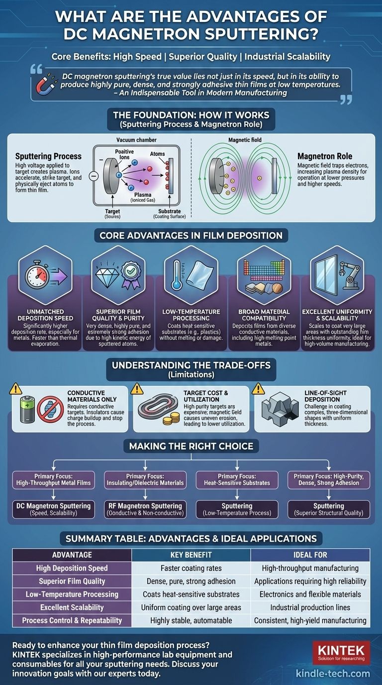
The core advantages of DC magnetron sputtering are its combination of high deposition speed, the superior quality of the resulting films, and its exceptional scalability for industrial production. This physical vapor deposition (PVD) technique uses a magnetic field to enhance the efficiency of the sputtering process, making it a cornerstone for creating thin films from conductive materials.
DC magnetron sputtering's true value lies not just in its speed, but in its ability to produce highly pure, dense, and strongly adhesive thin films at low temperatures. This unique combination of benefits makes it an indispensable tool in modern manufacturing, from semiconductors to architectural glass.
The Foundation: Why It's So Effective
To understand the advantages, it's helpful to grasp the core mechanism. Sputtering is a physical process, not a chemical or thermal one, which is the source of many of its benefits.
The Sputtering Process
In a vacuum chamber, a high voltage is applied to a source material, known as the target. This creates a plasma of ionized gas (typically argon). These positive ions are accelerated and collide with the negatively charged target, physically knocking off atoms.
These ejected atoms then travel through the chamber and deposit onto a substrate, forming a thin film.
The Role of the Magnetic Field
The "magnetron" part is the key innovation. A magnetic field is placed behind the target, which traps electrons from the plasma near the target's surface.
This electron trap dramatically increases the probability of collisions with argon gas atoms, creating a much denser plasma right where it's needed. This allows the process to run at lower pressures and higher speeds with less energy than non-magnetron sputtering.
Core Advantages in Film Deposition
The unique mechanism of magnetron sputtering directly leads to its primary benefits for producing high-quality thin films.
Unmatched Deposition Speed
The enhanced plasma density means more ions are available to strike the target. This results in a significantly higher deposition rate compared to other PVD techniques like thermal evaporation, especially for metals.
Superior Film Quality and Purity
Because sputtering is a physical ejection process, the resulting films are of exceptionally high quality. They are known for being very dense, highly pure, and having extremely strong adhesion to the substrate.
This is because sputtered atoms arrive at the substrate with much higher kinetic energy than evaporated atoms, which helps form a more robust film structure.
Low-Temperature Processing
The target material is not melted or evaporated. This means the overall process generates very little radiant heat, allowing for the coating of heat-sensitive substrates such as plastics and polymers without causing damage.
Broad Material Compatibility
Sputtering can be used to deposit films from a vast range of materials, including pure metals, alloys, and conductive compounds. It is particularly effective for high-melting-point materials that are difficult or impossible to deposit using thermal evaporation.
Built for Scale and Reliability
Beyond film quality, DC magnetron sputtering is engineered for the demands of modern industry.
Excellent Uniformity Over Large Areas
The process can be scaled to coat very large substrates—like architectural glass or flat-panel displays—with outstanding film thickness uniformity. This is critical for ensuring consistent performance and yield in high-volume manufacturing.
Repeatability and Automation
The parameters of the sputtering process (pressure, power, gas flow) are easily controlled. This leads to high process stability and repeatability, making it ideal for automation in a production line.
Understanding the Trade-offs
No technology is perfect. Objectivity requires acknowledging where DC magnetron sputtering has limitations.
The Conductive Material Limitation
DC (Direct Current) sputtering works by applying a static negative voltage to the target. If the target material is an insulator (a dielectric), positive charge will build up on its surface, quickly "poisoning" the target and stopping the process.
Therefore, DC magnetron sputtering is only suitable for conductive materials. To sputter insulators like silicon dioxide or aluminum oxide, a different technique like RF (Radio Frequency) sputtering is required.
Target Cost and Utilization
High-purity sputtering targets can be expensive. Furthermore, the magnetic field that enhances the process also causes the target to erode unevenly, typically in a "racetrack" pattern. This means not all of the costly target material can be used.
Line-of-Sight Deposition
Like most PVD processes, sputtering is largely a line-of-sight technique. While sputtered atoms have enough energy for some surface mobility, coating highly complex, three-dimensional shapes with uniform thickness can be challenging.
Making the Right Choice for Your Goal
Selecting the right deposition method depends entirely on your material and application goals.
- If your primary focus is high-throughput manufacturing of metal films: DC magnetron sputtering is the industry standard due to its unmatched speed, scalability, and process control.
- If your primary focus is depositing insulating or dielectric materials: You must use RF magnetron sputtering, as DC sputtering is fundamentally incompatible with non-conductive targets.
- If your primary focus is coating heat-sensitive substrates like plastics: The low-temperature nature of the sputtering process makes it a superior choice over thermal evaporation.
- If your primary focus is creating high-purity, dense films with strong adhesion: Sputtering's physical deposition mechanism produces films that are often superior in structural quality to evaporated films.
Ultimately, DC magnetron sputtering provides an unparalleled combination of speed, quality, and control for depositing conductive thin films in both research and high-volume production.
Summary Table:
| Advantage | Key Benefit | Ideal For |
|---|---|---|
| High Deposition Speed | Faster coating rates than other PVD methods | High-throughput manufacturing |
| Superior Film Quality | Dense, pure, and strongly adhesive films | Applications requiring high reliability |
| Low-Temperature Processing | Coats heat-sensitive substrates (e.g., plastics) | Electronics and flexible materials |
| Excellent Scalability | Uniform coating over large areas (e.g., architectural glass) | Industrial production lines |
| Process Control & Repeatability | Highly stable and automatable process | Consistent, high-yield manufacturing |
Ready to enhance your thin film deposition process? KINTEK specializes in providing high-performance lab equipment and consumables for all your sputtering needs. Whether you are in semiconductor manufacturing, research, or producing advanced coatings, our expertise ensures you achieve superior film quality, efficiency, and scalability. Contact our experts today to discuss how our solutions can power your innovation and production goals.
Visual Guide
Related Products
- Microwave Plasma Chemical Vapor Deposition MPCVD Machine System Reactor for Lab and Diamond Growth
- Laboratory CVD Boron Doped Diamond Materials
- 915MHz MPCVD Diamond Machine Microwave Plasma Chemical Vapor Deposition System Reactor
- Boron Nitride (BN) Ceramic Plate
- Molybdenum Tungsten Tantalum Special Shape Evaporation Boat
People Also Ask
- What pressure is needed for chemical vapor deposition of diamonds? Master the Low-Pressure 'Sweet Spot'
- How does MPCVD work? A Guide to Low-Temperature, High-Quality Film Deposition
- How do vacuum pumps and valves collaborate in MPCVD? Achieve Precise Pressure Control for Superior CNT Synthesis
- How are CVD diamonds created? Discover the Science of Lab-Grown Diamond Precision
- Why is argon-rich gas phase chemistry used for UNCD growth? Unlock Precision Nano-Diamond Synthesis


