At its core, Electron Beam Physical Vapor Deposition (E-beam PVD) is chosen for its superior deposition speed, high material purity, and versatility in handling a wide range of materials. Compared to other methods like sputtering, it offers faster processing for batch production and can use less expensive source materials, making it a highly efficient choice for many high-volume commercial applications.
The central advantage of E-beam PVD lies in its ability to deliver high-purity, high-quality thin films at a rapid rate. This combination of speed and quality makes it an invaluable tool for manufacturing advanced optics, semiconductors, and wear-resistant coatings.
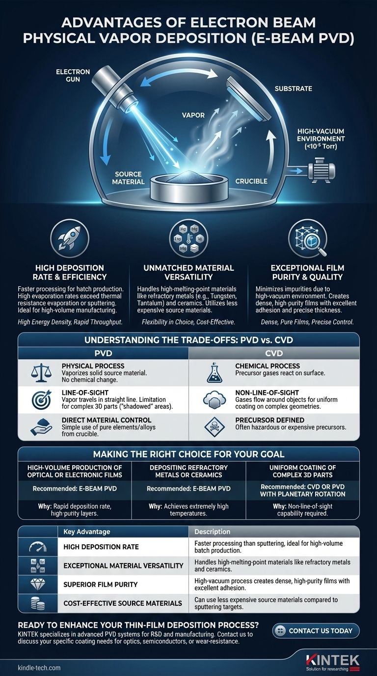
The Core Strengths of E-Beam PVD
Electron Beam PVD is a line-of-sight thermal evaporation process that uses a focused beam of high-energy electrons to vaporize a source material within a high-vacuum chamber. This vapor then travels and condenses onto a substrate, forming a thin film.
High Deposition Rate and Efficiency
E-beam PVD is known for being exceptionally fast. The high energy density of the electron beam allows for very high evaporation rates, far exceeding what is typically possible with other techniques like thermal resistance evaporation or sputtering.
This speed makes the process highly efficient and suitable for high-volume production runs, as it processes more rapidly in batch scenarios.
Unmatched Material Versatility
The process provides significant flexibility in material choice. Because the electron beam can generate intense, localized heat, it can evaporate materials with very high melting points and low vapor pressures, such as refractory metals (e.g., tungsten, tantalum) and ceramics.
Furthermore, E-beam PVD can utilize a wider array of less expensive evaporative source materials, as it doesn't require the specially fabricated, and often more costly, targets used in magnetron sputtering.
Exceptional Film Purity and Quality
The entire process takes place in a high-vacuum environment (typically 10⁻⁵ Torr or lower). This minimizes the presence of residual gases that could otherwise become incorporated into the film as impurities.
The result is the ability to create dense, highly pure thin films with excellent adhesion and precisely controlled thickness, critical for applications in optics and electronics.
Understanding the Trade-offs: PVD vs. CVD
To fully appreciate the advantages of E-beam PVD, it is useful to contrast it with Chemical Vapor Deposition (CVD), another common thin-film deposition method.
The Process Difference: Physical vs. Chemical
E-beam PVD is a physical process. It physically vaporizes a solid source material, which then deposits on the substrate without changing its chemical composition.
CVD is a chemical process. It introduces precursor gases into a chamber, which react and decompose on the substrate surface to form the desired film. This reliance on chemical reactions gives CVD its own unique set of capabilities.
The Line-of-Sight Limitation
E-beam PVD is a line-of-sight process. The vaporized material travels in a straight line from the source to the substrate. This is a key limitation when coating parts with complex, three-dimensional geometries, as "shadowed" areas will not be coated.
CVD, by contrast, is generally non-line-of-sight. The precursor gases can flow around an object, allowing for a highly uniform coating on all surfaces, even intricate internal ones.
Material Control and Cost
While both methods can produce high-purity films, PVD provides more direct control over depositing pure elements or alloys from a source crucible.
CVD processes are defined by the available chemical precursors, which can sometimes be hazardous or expensive. PVD's use of solid source materials is often simpler and more direct.
Making the Right Choice for Your Goal
Selecting the right deposition technology depends entirely on your specific application requirements for material, geometry, and production volume.
- If your primary focus is high-volume production of optical or electronic films: E-beam PVD is an excellent choice due to its rapid deposition rate and ability to produce high-purity layers.
- If your primary focus is depositing refractory metals or ceramics: E-beam PVD's ability to achieve extremely high temperatures makes it one of the few viable methods for these challenging materials.
- If your primary focus is uniform coating of complex 3D parts: You should strongly consider a non-line-of-sight method like CVD or use complex planetary rotation systems within your PVD chamber.
Ultimately, understanding these fundamental trade-offs empowers you to select the most effective and efficient technology for your specific manufacturing goal.
Summary Table:
| Key Advantage | Description |
|---|---|
| High Deposition Rate | Faster processing than sputtering, ideal for high-volume batch production. |
| Exceptional Material Versatility | Handles high-melting-point materials like refractory metals and ceramics. |
| Superior Film Purity | High-vacuum process creates dense, high-purity films with excellent adhesion. |
| Cost-Effective Source Materials | Can use less expensive source materials compared to sputtering targets. |
Ready to enhance your thin-film deposition process?
Electron Beam PVD is a powerful solution for applications demanding high purity and high throughput. KINTEK specializes in providing advanced lab equipment, including PVD systems, to meet the precise needs of laboratories in R&D and manufacturing.
Contact us today to discuss how our expertise and solutions can help you achieve superior coating results for your optics, semiconductor, or wear-resistant applications.
Visual Guide
Related Products
- Electron Beam Evaporation Coating Oxygen-Free Copper Crucible and Evaporation Boat
- Electron Beam Evaporation Coating Tungsten Crucible and Molybdenum Crucible for High Temperature Applications
- Electron Beam Evaporation Coating Gold Plating Tungsten Molybdenum Crucible for Evaporation
- Molybdenum Tungsten Tantalum Evaporation Boat for High Temperature Applications
- Electron Beam Evaporation Coating Conductive Boron Nitride Crucible BN Crucible
People Also Ask
- What is e-beam evaporation? Achieve High-Purity Thin Film Deposition for Your Lab
- What is e-beam evaporation used for? Precision Coating for Optics, Aerospace & Electronics
- What are the applications of e-beam evaporation? Achieve High-Purity Coatings for Optics & Electronics
- What is the container that holds the metal source material called in e-beam evaporation? Ensure Purity and Quality in Your Thin-Film Deposition
- What are the applications of electron beams? From Nanoscale Imaging to Industrial Manufacturing


