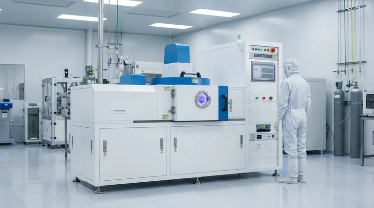
In the world of advanced material coating, the magnetron stands as a foundational technology for thin film deposition. Its core advantages are the ability to achieve high deposition rates while protecting the substrate from thermal damage. This is accomplished by using magnetic fields to trap electrons near the source material, which dramatically enhances the efficiency of the sputtering process and allows for the deposition of nearly any material, including complex alloys, without altering their composition.
The fundamental problem with basic sputtering is its inefficiency and the potential for substrate damage. Magnetron sputtering solves this by using a magnetic field to create a dense, localized plasma, leading to faster, safer, and more versatile material deposition.
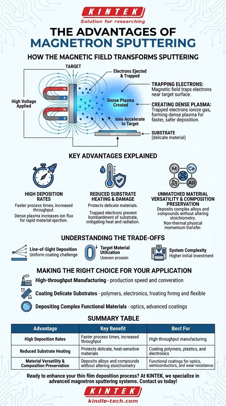
How the Magnetic Field Transforms Sputtering
At its heart, magnetron sputtering is an enhancement of a standard physical vapor deposition (PVD) process. The addition of a magnetic field is what provides its distinct advantages.
The Core Principle: Trapping Electrons
In a magnetron system, powerful magnets are placed behind the cathode, which is the block of source material you intend to deposit (known as the "target"). This creates a magnetic field that runs parallel to the target's surface.
When high voltage is applied, electrons are ejected from the target. Instead of flying directly to the substrate, they are trapped in a spiral path within the magnetic field, close to the target's surface.
Creating a Dense, Efficient Plasma
These trapped, spiraling electrons have a much longer path length. This drastically increases the probability that they will collide with and ionize neutral gas atoms (typically Argon) in the vacuum chamber.
This intense ionization creates a dense, stable plasma precisely where it is needed most: directly in front of the target. The resulting high concentration of positive ions then accelerates into the target, dislodging material far more effectively than in non-magnetron systems.
Key Advantages Explained
The efficiency gained by trapping electrons translates directly into several critical manufacturing and research benefits.
High Deposition Rates
Because the dense plasma creates a much higher flux of ions bombarding the target, material is ejected at a significantly faster rate. This leads to higher deposition rates on the substrate, shortening process times and increasing throughput in a production environment.
Reduced Substrate Heating and Damage
A key benefit of trapping electrons near the target is that they are prevented from bombarding the substrate. In other deposition methods, this electron bombardment can cause significant heating and radiation damage.
By mitigating this, magnetron sputtering is ideal for coating heat-sensitive materials like plastics, polymers, or delicate electronic components.
Unmatched Material Versatility
Magnetron sputtering is a non-thermal process; it does not rely on melting or evaporating the source material. Instead, it uses physical momentum transfer.
This means it can be used to deposit materials with extremely high melting points, such as tungsten or ceramics, that are difficult or impossible to deposit using thermal evaporation. It is compatible with nearly all metals, alloys, and compounds.
Preserving Complex Compositions
Since sputtering is a physical momentum-transfer process, it generally knocks atoms off the target in the same ratio as their composition.
This means if you use a target made of a specific alloy or compound, the resulting thin film will have the same stoichiometry (elemental ratio). This is crucial for creating films with specific functional properties, such as in semiconductors, optics, and wear-resistant coatings.
Understanding the Trade-offs
While powerful, magnetron sputtering is not without its operational considerations. Objectivity requires acknowledging its limitations.
Line-of-Sight Deposition
Like most PVD processes, magnetron sputtering is a "line-of-sight" technique. The sputtered material travels in a relatively straight line from the target to the substrate.
This can make it challenging to achieve a uniform coating on complex, three-dimensional shapes without sophisticated substrate rotation and planetary fixtures.
Target Material Utilization
The magnetic field that traps electrons often confines them to a specific region, leading to uneven erosion of the target material. This is often called a "racetrack."
This effect means that not all of the expensive target material is consumed, which can impact the cost-effectiveness of the process for very high-value materials.
System Complexity
A magnetron sputtering system is a sophisticated piece of equipment. It requires a high-vacuum chamber, precise gas flow controllers, high-power DC or RF power supplies, and cooling systems. The initial capital investment and operational complexity are higher than for simpler methods like electroplating or wet chemical deposition.
Making the Right Choice for Your Application
Selecting the right deposition technique depends entirely on your end goal. Magnetron sputtering excels in specific scenarios.
- If your primary focus is high-throughput manufacturing: The high deposition rates offer a significant advantage for production speed and cost-efficiency.
- If your primary focus is coating delicate substrates: The low thermal load makes it the superior choice for polymers, plastics, and sensitive electronic devices.
- If your primary focus is depositing complex functional materials: Its ability to preserve the stoichiometry of alloys and compounds is critical for performance in optics, electronics, and advanced coatings.
Magnetron sputtering's unique combination of speed, control, and material versatility makes it a cornerstone technology for modern materials science and manufacturing.
Summary Table:
| Advantage | Key Benefit | Best For |
|---|---|---|
| High Deposition Rates | Faster process times, increased throughput | High-throughput manufacturing |
| Reduced Substrate Heating | Protects delicate, heat-sensitive materials | Coating polymers, plastics, and electronics |
| Material Versatility & Composition Preservation | Deposits alloys and compounds without altering stoichiometry | Functional coatings for optics, semiconductors, and wear-resistance |
Ready to enhance your thin film deposition process?
At KINTEK, we specialize in advanced lab equipment, including magnetron sputtering systems designed for precision and reliability. Whether you're in research or manufacturing, our solutions help you achieve superior coating results with high efficiency and material integrity.
Contact us today to discuss how our expertise can meet your specific laboratory needs. Get in touch →
Visual Guide
Related Products
- Spark Plasma Sintering Furnace SPS Furnace
- RF PECVD System Radio Frequency Plasma-Enhanced Chemical Vapor Deposition RF PECVD
People Also Ask
- What are the fundamentals of spark plasma sintering process? Unlock Rapid, High-Performance Material Consolidation
- Why are Spark Plasma Sintering (SPS) furnaces or hot presses utilized in the preparation of Li3PS4 solid electrolytes?
- What is the mechanism of SPS process? A Deep Dive into Rapid, Low-Temperature Sintering
- What is the difference between spark plasma sintering and flash sintering? A Guide to Advanced Sintering Methods
- What is the pressure for spark plasma sintering? A Guide to Optimizing SPS Parameters

