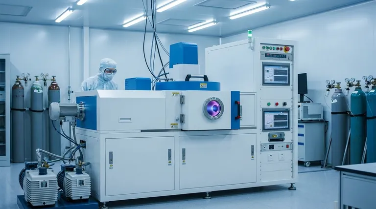
The primary advantage of RF sputtering is its unique ability to deposit thin films from non-conductive, insulating materials—a task that is fundamentally impossible for standard DC sputtering. This is achieved by using an alternating radio frequency field that prevents electrical charge from building up on the target surface, resulting in a more stable process, higher quality films, and greater material versatility.
While DC sputtering is a cost-effective workhorse for conductive metals, RF sputtering offers critical versatility. Its ability to handle insulating materials and operate at lower pressures unlocks the high-purity, uniform films that are essential for advanced electronics and optical coatings.

The Fundamental Difference: Handling Insulating Materials
The most significant distinction between RF and DC sputtering lies in the type of materials they can process. This limitation stems directly from the physics of how each method generates plasma.
The Problem with DC Sputtering and Insulators
In DC sputtering, a constant negative voltage is applied to a conductive target. This attracts positive gas ions (like Argon), which strike the target and eject atoms.
If you attempt this with an insulating (dielectric) target, the positive ions that strike the surface have nowhere to go. Their positive charge rapidly accumulates, neutralizing the negative voltage of the cathode and effectively repelling any more incoming ions, stopping the sputtering process entirely.
How RF Sputtering Solves the Charge Problem
RF sputtering replaces the direct current with a high-frequency alternating current (AC). This rapidly flips the target's potential between negative and positive.
During the negative half-cycle, the target attracts and is sputtered by positive ions, just like in DC sputtering. Crucially, during the positive half-cycle, the target attracts a flood of electrons from the plasma, which neutralizes the positive charge built up from the previous cycle. This allows the process to continue indefinitely without interruption.
Process Advantages of a Lower-Pressure Environment
Beyond material compatibility, RF sputtering's operating conditions create tangible benefits for the quality of the final thin film.
Increased Mean Free Path
RF sputtering can sustain a stable plasma at much lower working pressures (typically <15 mTorr) compared to DC sputtering (around 100 mTorr).
This lower pressure means there are far fewer gas atoms in the chamber. As a result, atoms ejected from the target travel to the substrate with fewer collisions, a concept known as a longer mean free path.
Higher Film Purity and Density
The direct path from target to substrate has a profound impact on film quality. Fewer collisions mean the sputtered atoms are less likely to be scattered or react with residual gas in the chamber, resulting in higher film purity.
Furthermore, because the atoms retain more of their initial kinetic energy, they create a denser and more adherent film when they arrive at the substrate.
Improved Process Stability
The charge neutralization mechanism inherent to RF sputtering eliminates the arcing that can plague DC systems, especially when dealing with reactive processes or target contamination. This leads to a more stable and repeatable deposition.
Additionally, the plasma in an RF system tends to encompass a larger area of the target. This reduces the concentrated "Race Track Erosion" common in DC systems, leading to more uniform target wear and a longer, more cost-effective target lifetime.
Understanding the Trade-offs: When DC Still Excels
Despite its significant advantages, RF sputtering is not always the superior choice. The objectivity required of a technical advisor demands acknowledging its limitations.
Slower Deposition Rates
Generally, RF sputtering has a slower deposition rate than DC sputtering for a given power input. The effective power delivered to the target can be roughly 50% of what a DC system provides, meaning it simply takes longer to deposit a film of the same thickness.
Higher Complexity and Cost
RF systems require more sophisticated equipment. An RF power supply and an impedance matching network are necessary to efficiently deliver power to the plasma, making the initial equipment investment significantly higher than for a simple DC power supply.
Increased Power Consumption
To achieve deposition rates comparable to DC sputtering, RF systems often require much higher power input. This translates directly to higher operational and energy costs, a critical factor in industrial-scale production.
Making the Right Choice for Your Application
The decision between RF and DC sputtering is not about a single "best" method, but about selecting the right tool for your specific goal.
- If your primary focus is cost-effective, high-rate deposition of conductive metals: DC sputtering is the clear and efficient choice.
- If you need to deposit insulating or dielectric materials (e.g., Al₂O₃, SiO₂, PZT): RF sputtering is not just an advantage; it is a fundamental requirement.
- If your goal is to produce the highest purity, densest films with superior uniformity: The low-pressure operation and stable plasma of RF sputtering make it the superior technical option, despite its higher cost.
Ultimately, understanding these core principles allows you to select the right sputtering technique not based on which is "better," but which is precisely suited to your material and performance goals.
Summary Table:
| Feature | RF Sputtering | DC Sputtering |
|---|---|---|
| Target Material | Conductive & Insulating (Dielectric) | Conductive Metals Only |
| Film Purity/Density | Higher (due to lower pressure) | Lower |
| Process Stability | High (prevents charge buildup) | Moderate (prone to arcing) |
| Deposition Rate | Slower | Faster |
| System Cost & Complexity | Higher | Lower |
Ready to Select the Perfect Sputtering System for Your Lab?
Choosing between RF and DC sputtering is critical for achieving your specific research or production goals. The experts at KINTEK specialize in lab equipment and consumables, serving all your laboratory needs. We can help you navigate these technical trade-offs to find the ideal solution for depositing high-quality thin films—whether you're working with advanced ceramics, optical coatings, or conductive metals.
Contact our specialists today to discuss your application and discover how KINTEK's expertise can enhance your lab's capabilities and efficiency.
Visual Guide

Related Products
- RF PECVD System Radio Frequency Plasma-Enhanced Chemical Vapor Deposition RF PECVD
- Horizontal High Temperature Graphite Vacuum Graphitization Furnace
- Spark Plasma Sintering Furnace SPS Furnace
- Automatic Laboratory Hydraulic Press for XRF & KBR Pellet Press
- Electron Beam Evaporation Coating Oxygen-Free Copper Crucible and Evaporation Boat
People Also Ask
- What is plasma enhanced chemical vapour deposition process? Unlock Low-Temperature, High-Quality Thin Films
- What is plasma enhanced chemical vapour deposition PECVD used for? Enable Low-Temp Thin Films for Electronics & Solar
- What is an example of PECVD? RF-PECVD for High-Quality Thin Film Deposition
- How does plasma enhance CVD? Unlock Low-Temperature, High-Quality Film Deposition
- How does Radio Frequency Enhanced Plasma Chemical Vapour Deposition (RF-PECVD) work? Learn the Core Principles


