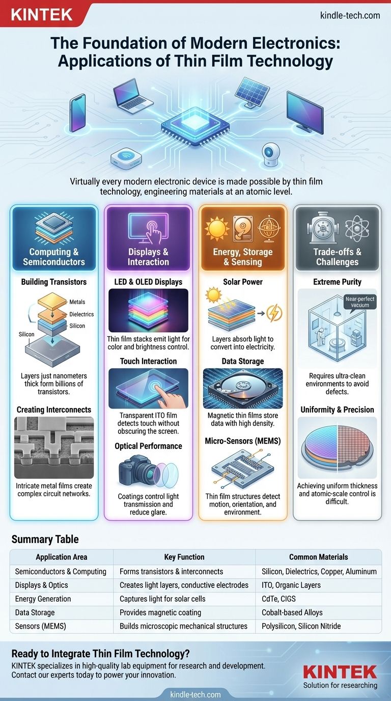
Virtually every modern electronic device you own is made possible by thin film technology. This foundational process is used to build the most critical components in our world, including the transistors in computer microprocessors, the light-emitting layers in LED and OLED displays, the sensors in our phones, and the energy-capturing surfaces of solar cells. Thin films are not a single application, but rather the fundamental manufacturing principle that enables the miniaturization and functionality of all modern electronics.
The core value of thin film technology lies in the ability to engineer materials at an almost atomic level. By depositing ultra-thin layers of specific materials, we gain precise control over the electrical, optical, and physical properties required to build complex micro-devices.
The Foundation of Modern Computing
The most significant application of thin film technology is in the fabrication of semiconductors, the brains behind every computer, phone, and smart device.
Building Transistors Layer by Layer
A modern microprocessor contains billions of microscopic switches called transistors. These are not carved from a single block but are built up by depositing a sequence of incredibly thin films of different materials—such as silicon, dielectrics for insulation, and metals for conductivity—onto a silicon wafer. Each layer is just a few nanometers thick.
Creating the Interconnects
Once the transistors are formed, they must be wired together to create a functional circuit. This is also achieved by depositing thin films of conductive metals, like aluminum or copper, in intricate patterns that form a multi-level network of microscopic wiring.
Powering Our Visual and Interactive World
From the screen you are reading this on to the camera that captures your photos, thin films are essential for controlling light and enabling interaction.
The Magic of LED and OLED Displays
Modern displays are constructed from a stack of thin films. In LED and OLED technology, specific layers are designed to emit light when an electrical current is applied. The thickness and composition of these films determine the color and brightness of each individual pixel.
Enabling Touch Interaction
The seemingly magical ability of a touch screen comes from a transparent, electrically conductive thin film. This layer, often made of Indium Tin Oxide (ITO), can detect the location of your finger by measuring the change in its electrical field, all without obscuring the display underneath.
Enhancing Optical Performance
The lenses in your smartphone camera or other optical devices are coated with multiple thin films. These anti-reflective coatings are engineered to control how light is transmitted and reflected, reducing glare and improving image clarity.
Energy, Storage, and Sensing
Thin film applications extend beyond computing and displays into critical areas like energy generation, data storage, and environmental sensing.
Capturing Solar Power
Thin-film solar cells are a prime example of this technology in action. They are made by depositing successive layers of photovoltaic materials onto a substrate. Each layer is optimized to absorb a different part of the solar spectrum, maximizing the conversion of light into electricity.
Revolutionizing Data Storage
The platters inside a hard disk drive are coated with a magnetic thin film. Data is stored by altering the magnetic orientation of microscopic regions on this film. The precision of this thin film layer is what determines the storage density of the drive.
Building Micro-Sensors (MEMS)
Micro-Electro-Mechanical Systems (MEMS) are microscopic devices that combine electronic and mechanical components. Built using thin film techniques, they act as the sensors in your phone for detecting motion (accelerometers), orientation (gyroscopes), and even changes in altitude.
Understanding the Trade-offs: The Challenge of Precision
While the applications are powerful, the process of creating thin films is extraordinarily demanding and represents a significant technical challenge.
The Need for Extreme Purity
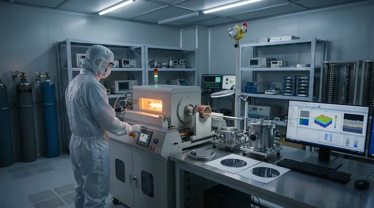
Thin film deposition must occur in a near-perfect vacuum. Any stray atoms or molecules can introduce defects into the film, ruining the performance of the final device. This requires complex and expensive equipment.
The Difficulty of Uniformity
Achieving a perfectly uniform film thickness across an entire surface—whether a 12-inch silicon wafer or a 65-inch display panel—is incredibly difficult. Variations of even a few atoms can lead to device failure, impacting manufacturing yield and cost.
Control at the Atomic Scale
The entire process hinges on controlling the deposition of material with atomic precision. This level of control requires sophisticated machinery and constant monitoring, making semiconductor and display fabrication one of the most capital-intensive industries in the world.
Making the Right Choice for Your Goal
Understanding the role of thin films is crucial for any professional working with modern technology, as the specific application directly shapes the engineering goal.
- If your primary focus is semiconductor design: Your goal is to use thin film deposition to create smaller, faster, and more power-efficient transistors and interconnects.
- If your primary focus is display technology: You are leveraging thin films to control light emission and conductivity with perfect uniformity and transparency.
- If your primary focus is energy systems: You are engineering multi-layered thin films to maximize photon absorption in solar cells or ion flow in advanced batteries.
- If your primary focus is sensors or MEMS: You rely on thin film deposition to build microscopic mechanical structures that can reliably respond to physical phenomena.
Ultimately, mastering thin film principles is equivalent to understanding the fundamental building blocks of our entire digital infrastructure.
Summary Table:
| Application Area | Key Function of Thin Film | Common Materials Used |
|---|---|---|
| Semiconductors & Computing | Forms transistors and interconnects on microchips. | Silicon, Dielectrics, Copper, Aluminum |
| Displays & Optics | Creates light-emitting layers (OLED/LED) and transparent conductive electrodes. | Indium Tin Oxide (ITO), Organic Layers |
| Energy Generation | Captures light in photovoltaic solar cells. | Cadmium Telluride (CdTe), CIGS |
| Data Storage | Provides magnetic coating for hard disk drive platters. | Cobalt-based Alloys |
| Sensors (MEMS) | Builds microscopic mechanical structures for motion and environmental sensing. | Polysilicon, Silicon Nitride |
Ready to Integrate Thin Film Technology into Your Lab's Workflow?
The applications of thin film deposition are vast, but achieving the required precision, purity, and uniformity requires reliable equipment. Whether you are developing next-generation semiconductors, advanced displays, or innovative sensors, the right tools are critical for success.
KINTEK specializes in providing high-quality lab equipment and consumables for all your thin film research and development needs. We understand the challenges of working at the atomic scale and can help you select the perfect solutions to enhance your project's yield and performance.
Let's discuss your specific application. Contact our experts today to find the equipment that will power your innovation.
Visual Guide
Related Products
- Aluminum-Plastic Flexible Packaging Film for Lithium Battery Packaging
- Thin-Layer Spectral Electrolysis Electrochemical Cell
People Also Ask
- How to tell if a lithium-ion battery is bad? Spot the critical signs of failure before it's too late.
- What is the thinnest coating? Unlocking Unique Properties at the Atomic Scale
- What is the difference between monolayer and multilayer film? Choose the Right Packaging for Your Product
- What are the properties of Aluminium (Al) relevant to its use in coatings? High Reflectivity & Conductivity Explored
- What is organic thin film? A Guide to Engineered Molecular Layers for Advanced Tech

