In modern electronics, semiconductor thin films are not merely a component; they are the fundamental building blocks of virtually all active devices. These precisely engineered layers, often just a few atoms thick, are directly responsible for the function of transistors, LEDs, sensors, and solar cells that power our world. Their applications range from the microprocessors in computer hardware to the displays on mobile phones.
At its core, the role of a thin film in a semiconductor is to create a region with specific electrical or optical properties. By stacking different types of these films, engineers can precisely control the flow of electrons and the interaction with light, which is the foundational principle behind every modern electronic device.
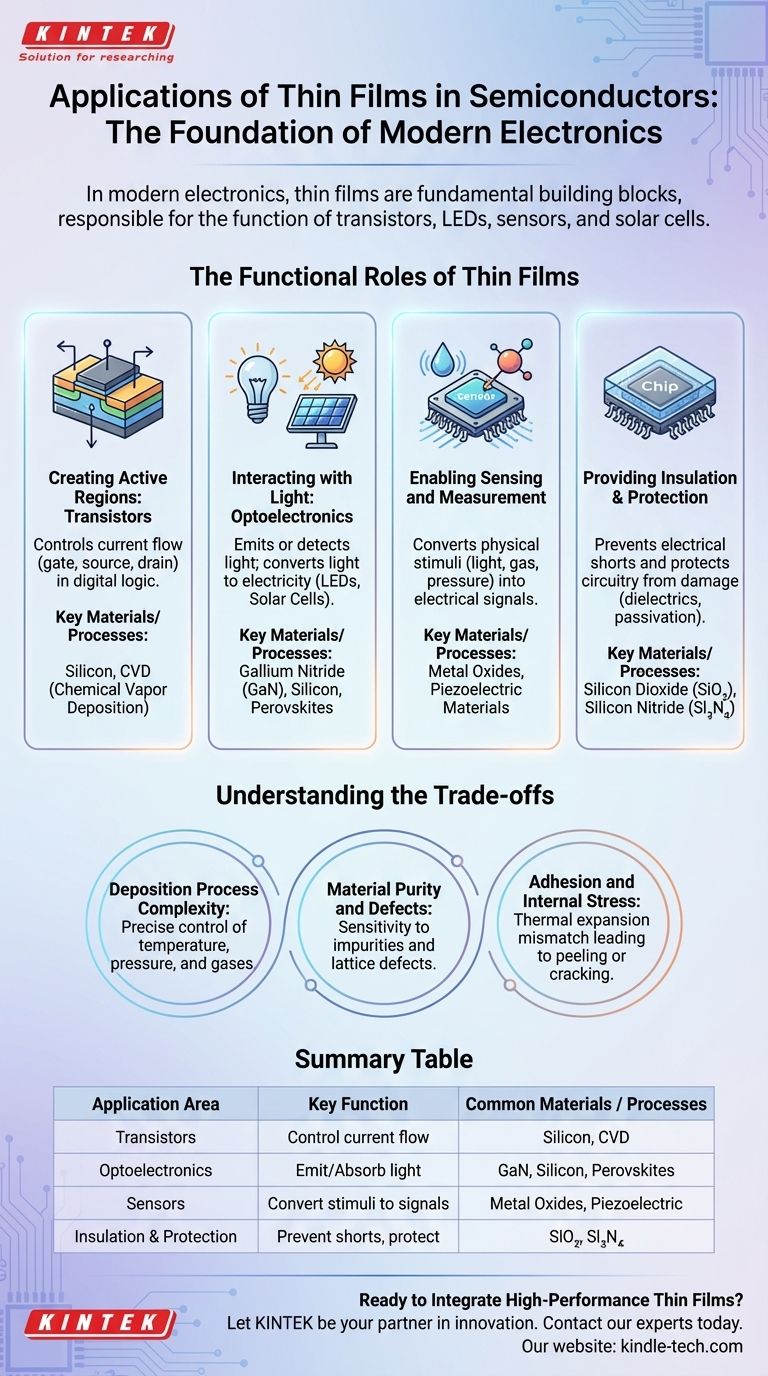
The Functional Roles of Thin Films
To understand the applications, you must first understand the function. A thin film's purpose is to manipulate energy—either electrical or light—at a microscopic scale. This is achieved through several key roles.
Creating the Active Regions: Transistors
The transistor is the elemental switch of all digital logic, from your phone to a supercomputer. A transistor works by controlling the flow of current through a channel.
These functional regions—the gate, source, and drain—are not carved from a block of silicon. Instead, they are built up by depositing a sequence of thin films, each with a specific composition and electrical property. Processes like Chemical Vapor Deposition (CVD) are used to grow these layers, atom by atom, onto a silicon wafer.
Interacting with Light: Optoelectronics
Many semiconductor devices are designed to either create or detect light. This entire field, known as optoelectronics, relies on the unique properties of specialized thin films.
For LEDs and displays, thin films are made from materials that emit photons (light) of a specific color when an electric current passes through them. For photovoltaic cells (solar panels), the opposite occurs: thin films are engineered to absorb photons from sunlight and generate an electrical current.
Enabling Sensing and Measurement
Thin films are also the active element in many types of sensors. The film is designed so that its electrical properties change predictably in response to an external stimulus.
This could be a change in light for an image sensor in a camera, a change in chemical composition for a gas detector, or a change in pressure for a micromachined pressure sensor. The thin film converts a physical phenomenon into a measurable electrical signal.
Providing Insulation and Protection
Not all films are electrically active. Some of the most critical layers in a microchip are insulators, also known as dielectrics.
These thin films prevent electrical current from leaking between adjacent wires or components, which would cause a short circuit. Other films serve as a final passivation layer, protecting the delicate circuitry from corrosion and physical damage.
Understanding the Trade-offs
Depositing and utilizing thin films is an incredibly precise and challenging process. The success of a multi-billion dollar fabrication plant hinges on controlling these layers perfectly.
Deposition Process Complexity
The final properties of a thin film are directly linked to its production method. Factors like temperature, pressure, and the purity of the chemical gases used in a CVD reactor must be controlled with extreme precision. A slight deviation can render millions of chips useless.
Material Purity and Defects
Semiconductor performance is exquisitely sensitive to impurities. A single misplaced atom in the crystal lattice of a thin film can create a defect that traps electrons, degrading or destroying the device's function. Achieving near-perfect crystalline structures across an entire wafer is a constant engineering battle.
Adhesion and Internal Stress
Stacking dozens of different materials, each with its own thermal expansion rate, creates immense internal stress. If the adhesion between film layers is poor, these stresses can cause the layers to peel apart (delamination) or crack, leading to immediate device failure.
Making the Right Choice for Your Goal
Understanding the role of thin films is essential for any professional working with electronic hardware. How you apply this knowledge depends on your specific focus.
- If your primary focus is device fabrication: The choice of deposition method and the rigorous control of process parameters are the most critical factors determining device performance and yield.
- If your primary focus is system integration: Understanding the function of each film type (active, optical, insulating) helps in selecting the right components and diagnosing failures in complex hardware.
- If your primary focus is research and development: The frontier lies in discovering novel thin film materials and deposition techniques to create more efficient solar cells, faster transistors, and entirely new types of sensors.
Ultimately, mastering the science of thin films is fundamental to advancing the capabilities of modern electronics.
Summary Table:
| Application Area | Key Function of Thin Film | Common Materials / Processes |
|---|---|---|
| Transistors | Create active regions (gate, source, drain) to control current flow. | Silicon, CVD (Chemical Vapor Deposition) |
| Optoelectronics (LEDs, Solar Cells) | Emit or absorb light; convert light to electricity and vice versa. | Gallium Nitride (GaN), Silicon, Perovskites |
| Sensors | Convert physical stimuli (light, gas, pressure) into electrical signals. | Metal Oxides, Piezoelectric Materials |
| Insulation & Protection | Prevent electrical shorts and protect delicate circuitry. | Silicon Dioxide (SiO₂), Silicon Nitride (Si₃N₄) |
Ready to Integrate High-Performance Thin Films into Your Lab's Workflow?
As you've seen, the precise application of thin films is fundamental to semiconductor success. KINTEK specializes in providing the high-purity lab equipment and consumables necessary for reliable thin film deposition and analysis. Whether you are in device fabrication, R&D, or system integration, our solutions help you achieve the material purity and process control critical for your projects.
Let KINTEK be your partner in innovation. Contact our experts today to discuss how our products can enhance your semiconductor research and development.
Visual Guide
Related Products
- Electron Beam Evaporation Coating Oxygen-Free Copper Crucible and Evaporation Boat
- Thin-Layer Spectral Electrolysis Electrochemical Cell
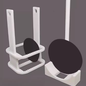
- Custom PTFE Wafer Holders for Lab and Semiconductor Processing
- Customizable PTFE Wafer Carriers for Semiconductor and Lab Applications
- Aluminum-Plastic Flexible Packaging Film for Lithium Battery Packaging
People Also Ask
- What is the container that holds the metal source material called in e-beam evaporation? Ensure Purity and Quality in Your Thin-Film Deposition
- How is an electron beam evaporator cooled during deposition? Essential Thermal Management for Stable Processes
- What is the temperature of e-beam evaporation? Mastering the Two-Zone Thermal Process for Precision Films
- What is the current of e-beam evaporation? A Guide to High-Purity Thin Film Deposition
- What are the applications of electron beams? From Nanoscale Imaging to Industrial Manufacturing