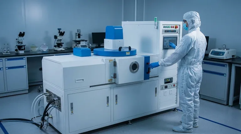
Working with thin films is a game of atomic-level precision. The core challenges revolve around controlling the film's structure, purity, and its physical relationship with the surface it's applied to. Key difficulties include achieving perfect thickness uniformity, ensuring the film adheres without peeling, managing internal stress that can cause cracking, and preventing microscopic contamination, all while trying to maintain a scalable and cost-effective process.
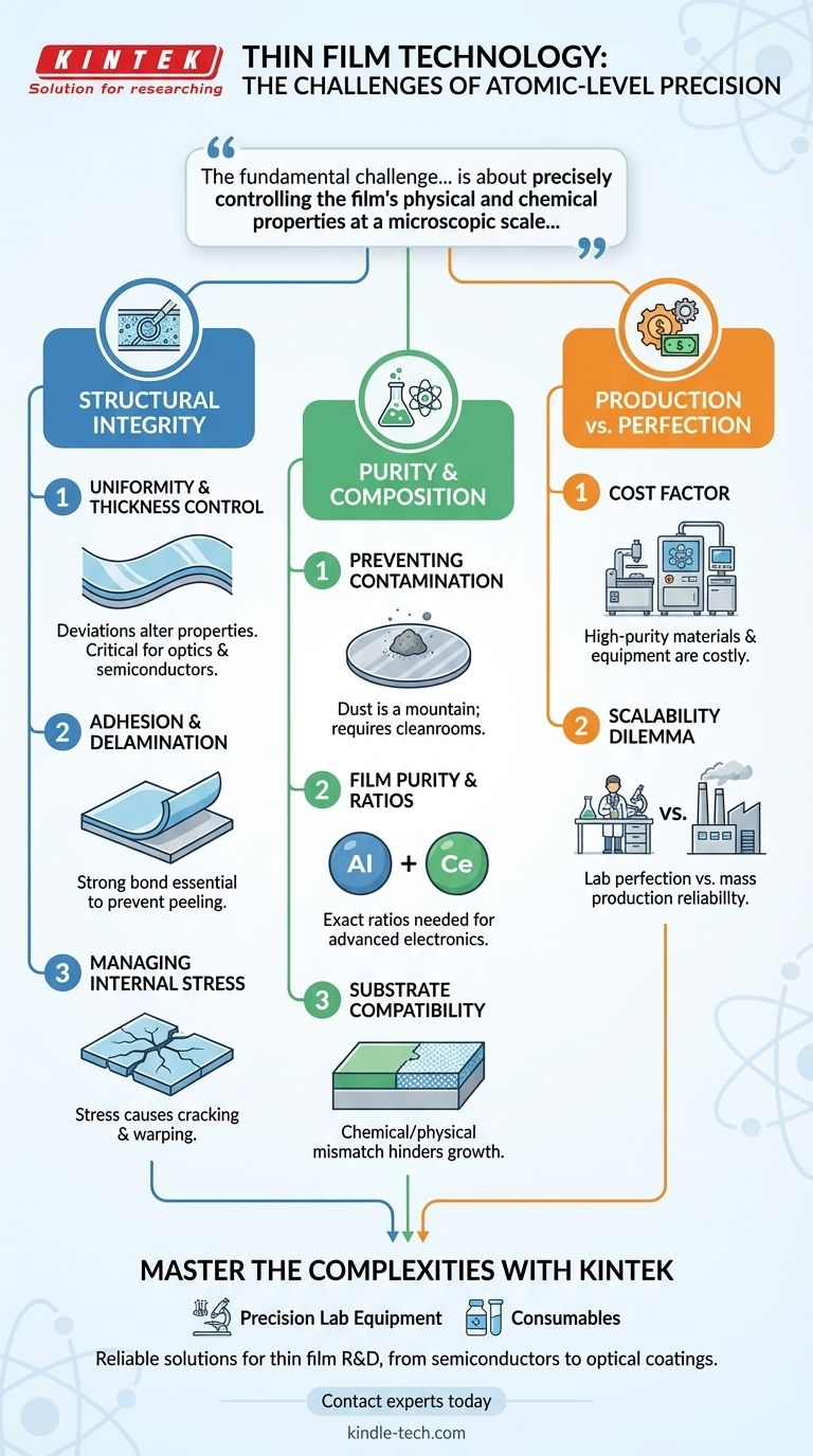
The fundamental challenge of thin film technology is not merely creating a thin layer of material. It is about precisely controlling the film's physical and chemical properties at a microscopic scale to ensure it performs reliably and consistently with its underlying substrate.
The Challenge of Structural Integrity
The physical structure of a thin film and its bond to the substrate determine its durability and performance. Flaws in this area are the most common points of failure.
Achieving Uniformity and Thickness Control
A film's properties are directly tied to its thickness. Even minuscule variations across a surface can completely alter its electrical, optical, or mechanical behavior.
In applications like optical coatings or semiconductors, a deviation of just a few nanometers can render a device useless.
Ensuring Proper Adhesion
The bond between the thin film and the substrate must be exceptionally strong. If the film doesn't adhere properly, it can peel or flake off, a failure known as delamination.
This is a critical concern for hard coatings on cutting tools or protective layers on electronics, where the film is subjected to physical stress.
Managing Internal Stress and Strain
Stress naturally builds within a film during the deposition process. This can be caused by a mismatch in the thermal expansion rates between the film and the substrate or by the deposition conditions themselves.
Excessive internal stress can cause the film to crack, warp, or lose adhesion, compromising the entire component.
The Challenge of Purity and Composition
The chemical makeup of the film is just as important as its physical structure. Contaminants or incorrect material ratios can completely negate the film's intended function.
Preventing Contamination
On the scale of thin films, a single speck of dust is a mountain. Any unwanted particle or chemical impurity can disrupt the film's growth, creating defects that undermine its performance.
This is why most thin film deposition occurs in highly controlled environments like cleanrooms or vacuum chambers.
Maintaining Film Purity and Composition
For films made of alloys or compound materials, achieving the exact chemical ratio is essential. This is particularly true for advanced electronics like LEDs or semiconductors.
A slight deviation in the composition can drastically change the material's properties, preventing it from functioning as designed.
Ensuring Substrate Compatibility
The substrate is not a passive surface; it is an active participant in the film's creation. The film material must be chemically and physically compatible with the surface it is being applied to.
Issues like poor chemical bonding or mismatched crystal structures can prevent the film from forming correctly, leading to poor adhesion and performance.
Understanding the Trade-offs: Production vs. Perfection
Achieving a flawless thin film in a lab is one thing; doing so repeatably for thousands of units is another. The practical challenges of manufacturing are significant.
The Cost Factor
The equipment needed for high-quality thin film deposition, such as vacuum systems, and the high-purity materials themselves are inherently expensive.
Balancing the required quality of the film with the cost of production is a constant engineering challenge.
The Scalability Dilemma
A process that creates a perfect film on a small laboratory sample may be difficult or economically unfeasible to scale up for mass production.
Engineers must constantly innovate to find deposition methods that are not only precise but also fast, reliable, and cost-effective at an industrial scale.
Prioritizing Your Efforts Based on Application
The most critical challenges depend entirely on the film's final use case.
- If your primary focus is optical coatings: Your success hinges on absolute precision in thickness control and uniformity to manage light reflection and transmission.
- If your primary focus is semiconductor devices: The non-negotiable factors are purity, preventing contamination, and precise composition to ensure correct electronic properties.
- If your primary focus is mechanical hard coatings: You must prioritize adhesion and managing internal stress to prevent delamination and cracking under physical load.
Success in thin film technology lies in mastering the delicate interplay between the material, the substrate, and the deposition process.
Summary Table:
| Challenge Category | Key Difficulties | Impact on Application |
|---|---|---|
| Structural Integrity | Uniformity, Adhesion, Internal Stress | Device failure, delamination, cracking |
| Purity & Composition | Contamination, Chemical Ratios, Substrate Compatibility | Unreliable performance, altered material properties |
| Production & Scalability | High Cost, Process Scalability | Economic feasibility for mass production |
Master the complexities of thin film deposition in your lab. The challenges of achieving perfect uniformity, adhesion, and purity require reliable, high-performance equipment. KINTEK specializes in precision lab equipment and consumables for all your thin film research and development needs.
Contact our experts today to find the right solution for your specific application, whether it's for semiconductors, optical coatings, or mechanical hard coatings.
Visual Guide
Related Products
- Aluminized Ceramic Evaporation Boat for Thin Film Deposition
- Tungsten Evaporation Boat for Thin Film Deposition
- Electron Beam Evaporation Coating Oxygen-Free Copper Crucible and Evaporation Boat
- Molybdenum Tungsten Tantalum Evaporation Boat for High Temperature Applications
- Aluminum-Plastic Flexible Packaging Film for Lithium Battery Packaging
People Also Ask
- What are the alternatives to sputtering? Choose the Right Thin Film Deposition Method
- Why are high-purity ceramic boats used for lignin activation? Ensure Purity & Thermal Stability
- What are thin films deposited by evaporation? A Guide to High-Purity Coating
- What is the source of evaporation for thin film? Choosing Between Thermal and E-Beam Methods
- What are the applications of thin films deposition? Unlock New Possibilities for Your Materials


