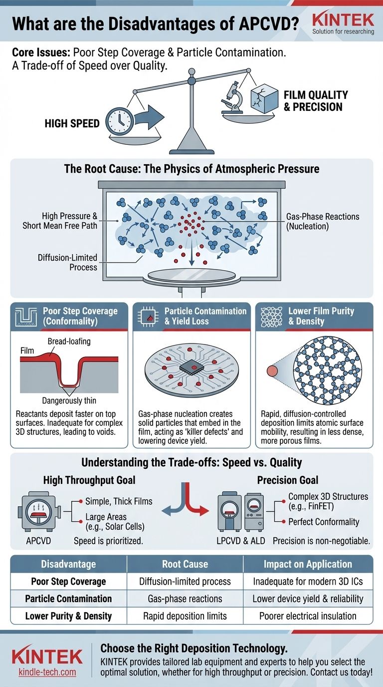
At its core, the primary disadvantages of Atmospheric Pressure Chemical Vapor Deposition (APCVD) are its poor step coverage (conformality) and a higher potential for particle contamination. These issues stem directly from its defining characteristic—operating at atmospheric pressure—which favors high deposition speed at the expense of film quality and precision.
APCVD is a technology of trade-offs. It offers exceptional throughput and simplicity, making it ideal for some applications. However, the fundamental physics of its high-pressure process make it unsuitable for the complex, high-aspect-ratio structures required in modern integrated circuits.
The Root Cause: The Physics of Atmospheric Pressure
To understand APCVD's limitations, we must first understand why operating at atmospheric pressure is so different from low-pressure (LPCVD) or vacuum-based methods.
High Pressure and Short Mean Free Path
At atmospheric pressure, the deposition chamber is dense with gas molecules. This dramatically reduces the mean free path—the average distance a reactant molecule can travel before colliding with another.
These frequent collisions mean the process is diffusion-limited. Reactants arrive at the wafer surface in a chaotic, non-uniform way, dictated more by concentration gradients than by a controlled surface reaction.
The Problem of Gas-Phase Reactions
The high concentration of precursor gases also increases the likelihood of reactions occurring in the gas phase, before the molecules even reach the substrate.
These gas-phase reactions form tiny solid particles (nucleation) that can then fall onto the wafer surface, creating significant defects and compromising device reliability.
Key Disadvantages Explained
The physics of the high-pressure environment leads directly to several critical operational disadvantages.
Poor Step Coverage (Conformality)
Step coverage refers to a film's ability to evenly coat a surface with complex topography, like trenches or vias. APCVD's performance here is notoriously poor.
Because the process is diffusion-limited, reactants deposit much faster on the top horizontal surfaces than they can diffuse down into deep, narrow features. This results in a thick film at the top and a dangerously thin or non-existent film at the bottom, a phenomenon known as "bread-loafing." This is a fatal flaw for creating modern, high-density circuits.
Particle Contamination and Yield Loss
As mentioned, gas-phase nucleation is a significant issue. These particles become embedded in the growing film, acting as killer defects that can short-circuit a transistor or break a connection.
This inherent tendency toward particle formation makes APCVD a higher-risk process for applications where pristine, defect-free films are non-negotiable, directly impacting manufacturing yield.
Lower Film Purity and Density
The rapid, diffusion-controlled deposition rate of APCVD gives atoms less time and surface mobility to arrange themselves into a dense, ordered film structure.
This can result in films that are less dense, more porous, and potentially contain more impurities compared to films grown with slower, more controlled methods like LPCVD. For critical dielectric layers, this can lead to poor electrical insulation and reliability issues.
Understanding the Trade-offs: Speed vs. Quality
It is crucial to view APCVD not as an inferior technology, but as a specialized tool where speed is prioritized over precision.
When High Throughput is the Goal
APCVD excels at depositing thick films quickly and inexpensively over large areas. This makes it a viable choice for applications where perfect conformality and ultra-low defect counts are not the primary concerns.
Examples include thick oxide layers for some solar cells, passivation layers on simpler devices, or pre-metal dielectrics (PMD) in older semiconductor manufacturing nodes.
When Precision is Non-Negotiable
For modern microelectronics, the game is about precision. Creating the complex 3D structures of FinFET transistors or deep memory trenches requires near-perfect conformality.
In these cases, the poor step coverage of APCVD is a disqualifying factor. Technologies like LPCVD and especially Atomic Layer Deposition (ALD), which rely on surface-reaction-limited kinetics, are the required choice, despite their slower deposition rates.
Making the Right Choice for Your Goal
Selecting a deposition method requires aligning the process capabilities with the end-goal requirements.
- If your primary focus is high-volume production of simple, thick films: APCVD's exceptional deposition rate and operational simplicity make it a strong and cost-effective candidate.
- If your primary focus is creating highly conformal films for advanced microelectronics: The poor step coverage of APCVD makes it unsuitable; you must use a low-pressure method like LPCVD or ALD.
- If your primary focus is maximizing device yield by minimizing defects: The inherent risk of particle contamination from gas-phase reactions makes APCVD a less desirable choice than vacuum-based systems.
Ultimately, understanding the fundamental trade-off between deposition speed and film precision is the key to selecting the most effective technology for your specific application.
Summary Table:
| Disadvantage | Root Cause | Impact on Application |
|---|---|---|
| Poor Step Coverage (Conformality) | Diffusion-limited process at high pressure | Inadequate coating for complex 3D structures in modern ICs |
| High Particle Contamination | Gas-phase reactions due to high precursor concentration | Lower device yield and reliability issues |
| Lower Film Purity & Density | Rapid deposition limits atomic surface mobility | Poorer electrical insulation and film integrity |
Need to choose the right deposition technology for your lab's specific requirements? At KINTEK, we specialize in providing tailored lab equipment and consumables for all your deposition needs. Whether you're prioritizing high throughput with APCVD or require the precision of LPCVD/ALD systems, our experts can help you select the optimal solution to maximize your research and production outcomes. Contact us today to discuss your project and discover how KINTEK can enhance your laboratory's capabilities!
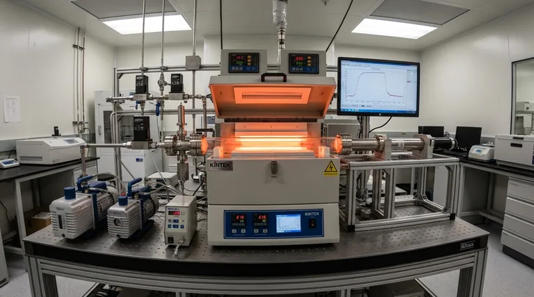
Visual Guide
Related Products
- Inclined Rotary Plasma Enhanced Chemical Vapor Deposition PECVD Equipment Tube Furnace Machine
- Multi Heating Zones CVD Tube Furnace Machine Chemical Vapor Deposition Chamber System Equipment
- Chemical Vapor Deposition CVD Equipment System Chamber Slide PECVD Tube Furnace with Liquid Gasifier PECVD Machine
- Inclined Rotary Plasma Enhanced Chemical Vapor Deposition PECVD Equipment Tube Furnace Machine
- RF PECVD System Radio Frequency Plasma-Enhanced Chemical Vapor Deposition RF PECVD
People Also Ask
- Why is a PECVD system required for vertical graphene synthesis? Master Directional Control for 3D Nanostructures
- What are the core advantages of PE-CVD in OLED encapsulation? Protect Sensitive Layers with Low-Temp Film Deposition
- What are the benefits of plasma enhanced CVD? Achieve High-Quality, Low-Temperature Film Deposition
- What is the necessity of depositing a silicon nitride (SiNx) thin film using PECVD? Optimize QSSPC Lifetime Measurement
- What is plasma enhanced chemical vapor deposition PECVD equipment? A Guide to Low-Temperature Thin Film Deposition


