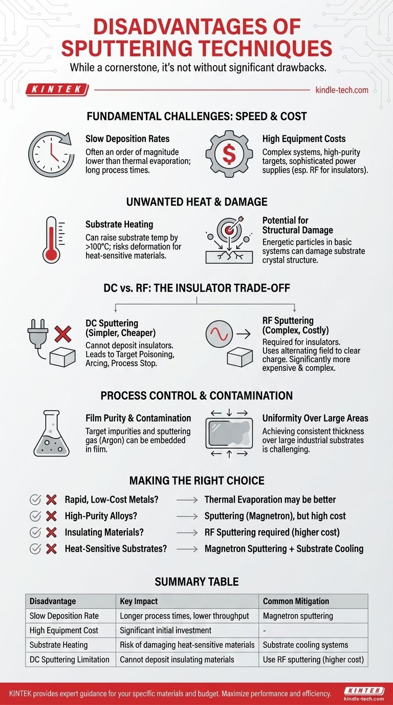
While a cornerstone of modern thin-film deposition, the sputtering process is not without significant drawbacks. Its primary disadvantages are relatively slow deposition rates, high initial equipment costs, the potential for unwanted substrate heating, and material-specific limitations that dictate which sputtering technique can be used. These factors require careful consideration when evaluating sputtering against other deposition methods.
Sputtering is not a single process but a family of techniques. Its most cited disadvantages—slow speed and potential heat damage—are most severe in basic diode systems. Advanced methods mitigate these issues but introduce a direct trade-off between performance, system complexity, and cost.
The Fundamental Challenges: Speed and Efficiency
The most universal criticisms of sputtering relate to its inherent speed and cost, especially when compared to methods like thermal evaporation.
Slow Deposition Rates
Sputtering is a physical, momentum-transfer process, which is fundamentally less efficient at depositing material than melting a source. This results in deposition rates that are often an order of magnitude lower than thermal evaporation techniques.
This slower speed translates directly to longer process times, which can be a significant bottleneck in high-volume manufacturing environments.
High Equipment and Operational Costs
Sputtering systems are complex and expensive. They require a high-vacuum chamber, costly high-purity target materials, and sophisticated power supplies.
The cost is further amplified when depositing insulating materials, which requires a more complex and expensive Radio Frequency (RF) power supply instead of a simpler Direct Current (DC) one.
The Problem of Unwanted Heat and Damage
The plasma environment that drives the sputtering process can also be a source of significant problems for the material being coated.
Substrate Heating
The substrate is subjected to heat from multiple sources, most notably the condensation of sputtered atoms and bombardment by high-energy electrons from the plasma.
This can easily raise the substrate temperature by over 100°C. For heat-sensitive substrates like polymers or certain semiconductor devices, this can cause deformation, degradation, or complete failure.
Potential for Structural Damage
Beyond just heat, the energetic particle bombardment in basic diode sputtering can cause direct damage to the substrate's crystal structure. This is a critical concern in applications like microelectronics where the substrate's integrity is paramount.
Advanced techniques like magnetron sputtering are specifically designed to confine the damaging electrons near the target, largely mitigating this issue.
Understanding the Trade-offs: DC vs. RF Sputtering
A major disadvantage emerges when you need to deposit materials that do not conduct electricity. The choice between DC and RF sputtering introduces a critical trade-off.
The Limitation of DC Sputtering: Insulators
DC sputtering, the simpler and cheaper method, works only for conductive targets. If you attempt to sputter an insulating material (like a ceramic oxide), positive ions build up on the target's surface.
This charge buildup, known as target poisoning, eventually repels the incoming argon ions, leading to process instabilities like arcing and ultimately stopping the deposition process entirely.
The RF Sputtering Solution and its Cost
To deposit insulators, RF sputtering is required. It uses an alternating electric field that effectively clears the positive charge buildup from the target on each cycle, allowing the process to continue.
However, RF power supplies and their associated matching networks are significantly more expensive and complex than their DC counterparts, representing a major disadvantage in cost and system maintenance.
Process Control and Contamination Risks
Even in a well-controlled system, sputtering presents potential challenges to film quality and scalability.
Film Purity and Contamination
While known for high-purity films, sputtering is not immune to contamination. Impurities within the source target material can be transferred to the thin film. The sputtering gas itself (typically Argon) can also become embedded in the growing film, which can be undesirable for certain applications.
Uniformity Over Large Areas
Sputtering provides excellent uniformity on a small scale. However, achieving that same level of thickness uniformity over very large industrial substrates (e.g., architectural glass) can be challenging.
Large rectangular cathodes can suffer from uneven plasma density, which directly impacts the deposition rate and leads to variations in film thickness across the substrate.
Making the Right Choice for Your Application
The "best" deposition method depends entirely on balancing these disadvantages against your project's specific needs.
- If your primary focus is rapid, low-cost deposition of simple metals: Sputtering's slow rate and high cost are key disadvantages, and a simpler method like thermal evaporation may be a better fit.
- If your primary focus is depositing high-purity alloy or refractory metal films: The precise stoichiometric control of sputtering often outweighs its slower speed, but you must be prepared for the high equipment cost.
- If your primary focus is coating insulating materials like oxides or nitrides: You must budget for an RF sputtering system, as DC sputtering is simply not a viable option for these materials.
- If your primary focus is coating heat-sensitive substrates like polymers: You must prioritize systems with effective substrate cooling and use magnetron sputtering to minimize direct plasma-induced damage.
By understanding these inherent limitations, you can accurately weigh the costs and benefits to select the right deposition technology for your goal.
Summary Table:
| Disadvantage | Key Impact | Common Mitigation |
|---|---|---|
| Slow Deposition Rate | Longer process times, lower throughput | Magnetron sputtering |
| High Equipment Cost | Significant initial investment | |
| Substrate Heating | Risk of damaging heat-sensitive materials | Substrate cooling systems |
| DC Sputtering Limitation | Cannot deposit insulating materials | Use RF sputtering (higher cost) |
Navigating the trade-offs of thin-film deposition is complex. KINTEK specializes in lab equipment and consumables, providing expert guidance to help you select the ideal sputtering system for your specific materials and budget. Let our team help you maximize performance and efficiency—contact us today for a consultation!
Visual Guide
Related Products
- RF PECVD System Radio Frequency Plasma-Enhanced Chemical Vapor Deposition RF PECVD
- Chemical Vapor Deposition CVD Equipment System Chamber Slide PECVD Tube Furnace with Liquid Gasifier PECVD Machine
- Electron Beam Evaporation Coating Oxygen-Free Copper Crucible and Evaporation Boat
- Aluminized Ceramic Evaporation Boat for Thin Film Deposition
- Hemispherical Bottom Tungsten Molybdenum Evaporation Boat
People Also Ask
- What are the benefits of PECVD? Achieve Superior Low-Temperature Thin Film Deposition
- What is an example of PECVD? RF-PECVD for High-Quality Thin Film Deposition
- What is plasma activated chemical vapour deposition method? A Low-Temperature Solution for Advanced Coatings
- How are PECVD and CVD different? A Guide to Choosing the Right Thin-Film Deposition Process
- What is the principle of plasma enhanced chemical vapor deposition? Achieve Low-Temperature Thin Film Deposition