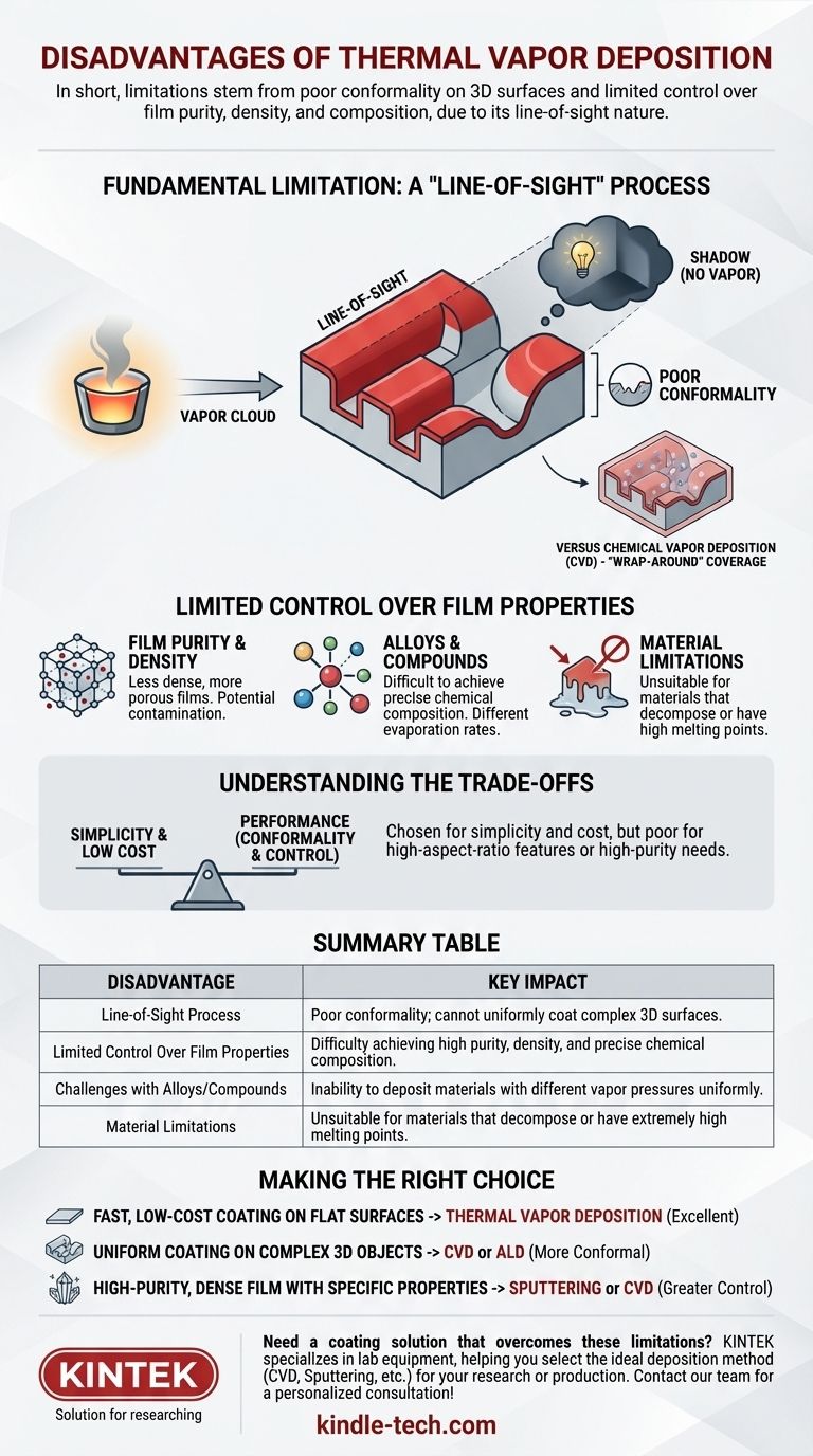
In short, the primary disadvantages of thermal vapor deposition are its poor ability to uniformly coat complex, three-dimensional surfaces and the limited control it offers over the final film's purity, density, and chemical composition. This is because it is a "line-of-sight" physical process, unlike the more versatile chemical reaction-based methods.
While valued for its simplicity and low cost, thermal vapor deposition's core limitations are tied directly to its mechanism. The process struggles to coat anything but the directly exposed surfaces of a substrate, and it provides fewer ways to fine-tune the structural and chemical properties of the resulting film.
The Fundamental Limitation: A "Line-of-Sight" Process
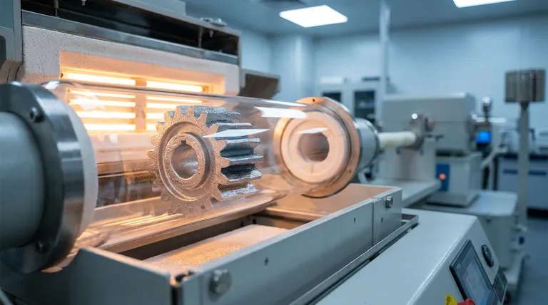
The most significant drawback of thermal vapor deposition stems from how the material travels from the source to the substrate. The process involves heating a material in a vacuum until it evaporates, creating a vapor cloud that then condenses on the cooler substrate.
What "Line-of-Sight" Means
The vaporized atoms travel in straight lines from the evaporation source to the substrate. Think of it like a lightbulb in a dark room—only the surfaces directly facing the bulb are illuminated. Any surface in a "shadow" receives little to no vapor.
The Consequence: Poor Conformality
This "line-of-sight" nature results in poor conformality, which is the ability to deposit a film of uniform thickness on a non-flat surface. While a flat wafer facing the source will be coated evenly, a complex object with trenches, steps, or curves will have thick deposits on top and very thin or no deposits on the sidewalls and in the crevices.
This stands in stark contrast to Chemical Vapor Deposition (CVD), where a reactive gas fills the entire chamber and reacts on all heated surfaces, providing excellent "wrap-around" coverage.
Limited Control Over Film Properties
The simplicity of thermal evaporation is also its weakness. The process is primarily controlled by temperature and pressure, offering fewer "knobs to turn" to manage the final film quality compared to more advanced techniques.
Difficulty with Film Purity and Density
The film is created by simple condensation. This can lead to films that are less dense and have a more porous or disordered crystal structure than those created by higher-energy or chemical processes. Furthermore, materials from the heating element or crucible can sometimes contaminate the film.
Challenges with Alloys and Compounds
Creating a film with a precise chemical composition of multiple elements (an alloy) is extremely difficult with thermal evaporation. Different materials have different vapor pressures, meaning they will evaporate at different rates at the same temperature. The result is a film whose composition changes during the deposition and rarely matches the source material.
Inability to Deposit Certain Materials
Materials that do not melt and evaporate cleanly are unsuitable for thermal deposition. Some materials decompose when heated, while others (refractory metals like tungsten) have such high melting points that evaporating them is impractical and energy-intensive.
Understanding the Trade-offs: Simplicity vs. Performance
No deposition technique is perfect; the choice depends entirely on the goal. Thermal vapor deposition's disadvantages must be weighed against its significant advantages.
The Power of Simplicity and Cost
The primary reason thermal vapor deposition is so widely used is because it is often the cheapest, fastest, and simplest method available. The equipment is relatively straightforward and easy to operate and maintain, making it ideal for research and applications where perfect conformality or film structure is not the top priority.
When to Avoid Thermal Deposition
You should avoid this method if your application requires a uniform coating on a high-aspect-ratio feature, like the inside of a deep trench in a microchip. It is also a poor choice when you need a film with exceptionally high purity, specific crystalline orientation, or a precisely controlled alloy composition.
Making the Right Choice for Your Goal
Selecting the correct deposition method requires understanding your primary objective.
- If your primary focus is a fast, low-cost coating on a relatively flat surface: Thermal vapor deposition is an excellent and highly effective choice.
- If your primary focus is a uniform, pinhole-free coating on a complex 3D object: You must use a more conformal method, like Chemical Vapor Deposition (CVD) or Atomic Layer Deposition (ALD).
- If your primary focus is a high-purity, dense film with specific structural or chemical properties: Other methods like sputtering (another type of PVD) or CVD offer far greater control over the final product.
Ultimately, understanding the trade-offs between the simplicity of thermal evaporation and the high performance of chemical methods empowers you to select the right tool for the job.
Summary Table:
| Disadvantage | Key Impact |
|---|---|
| Line-of-Sight Process | Poor conformality; cannot uniformly coat complex 3D surfaces or trenches. |
| Limited Control Over Film Properties | Difficulty achieving high purity, density, and precise chemical composition. |
| Challenges with Alloys/Compounds | Inability to deposit materials with different vapor pressures uniformly. |
| Material Limitations | Unsuitable for materials that decompose or have extremely high melting points. |
Need a coating solution that overcomes these limitations?
Thermal vapor deposition is not the right tool for every job. If your project requires uniform coatings on complex 3D structures, high-purity films, or precise material compositions, you need a more advanced solution.
KINTEK specializes in lab equipment and consumables, serving all your laboratory needs. Our experts can help you select the ideal deposition method—whether it's Chemical Vapor Deposition (CVD), sputtering, or another technique—to ensure your research or production achieves the desired results.
Let's find the right tool for your specific application. Contact our team today for a personalized consultation!
Visual Guide
Related Products
- CVD Diamond for Thermal Management Applications
- HFCVD Machine System Equipment for Drawing Die Nano-Diamond Coating
- Molybdenum Tungsten Tantalum Evaporation Boat for High Temperature Applications
- Aluminized Ceramic Evaporation Boat for Thin Film Deposition
- Chemical Vapor Deposition CVD Equipment System Chamber Slide PECVD Tube Furnace with Liquid Gasifier PECVD Machine
People Also Ask
- How do they make diamonds in CVD? Unlock the Secrets of Lab-Grown Diamond Creation
- What is the hardness of CVD diamond? The Ultimate Guide to Engineered Super-Materials
- Are CVD diamonds real or fake? Discover the Truth About Lab-Grown Diamonds
- How long does it take to grow a CVD diamond? A 2-4 Week Journey to a Flawless Gem
- Will a CVD diamond pass a diamond tester? Yes, because it's a real diamond.


