At its core, magnetron sputtering is a highly efficient physical vapor deposition (PVD) technique that uses a magnetic field to dramatically increase the rate at which a thin film is deposited onto a substrate. Its primary effects are the creation of dense, well-adhered coatings with precise thickness control, making it a cornerstone of modern industrial manufacturing for everything from microelectronics to wear-resistant tools.
The central effect of magnetron sputtering is a significant enhancement of the coating process. By using magnets to confine electrons near the target material, it achieves faster deposition rates and higher quality films at lower pressures than standard sputtering, but introduces trade-offs related to substrate heating and material limitations.
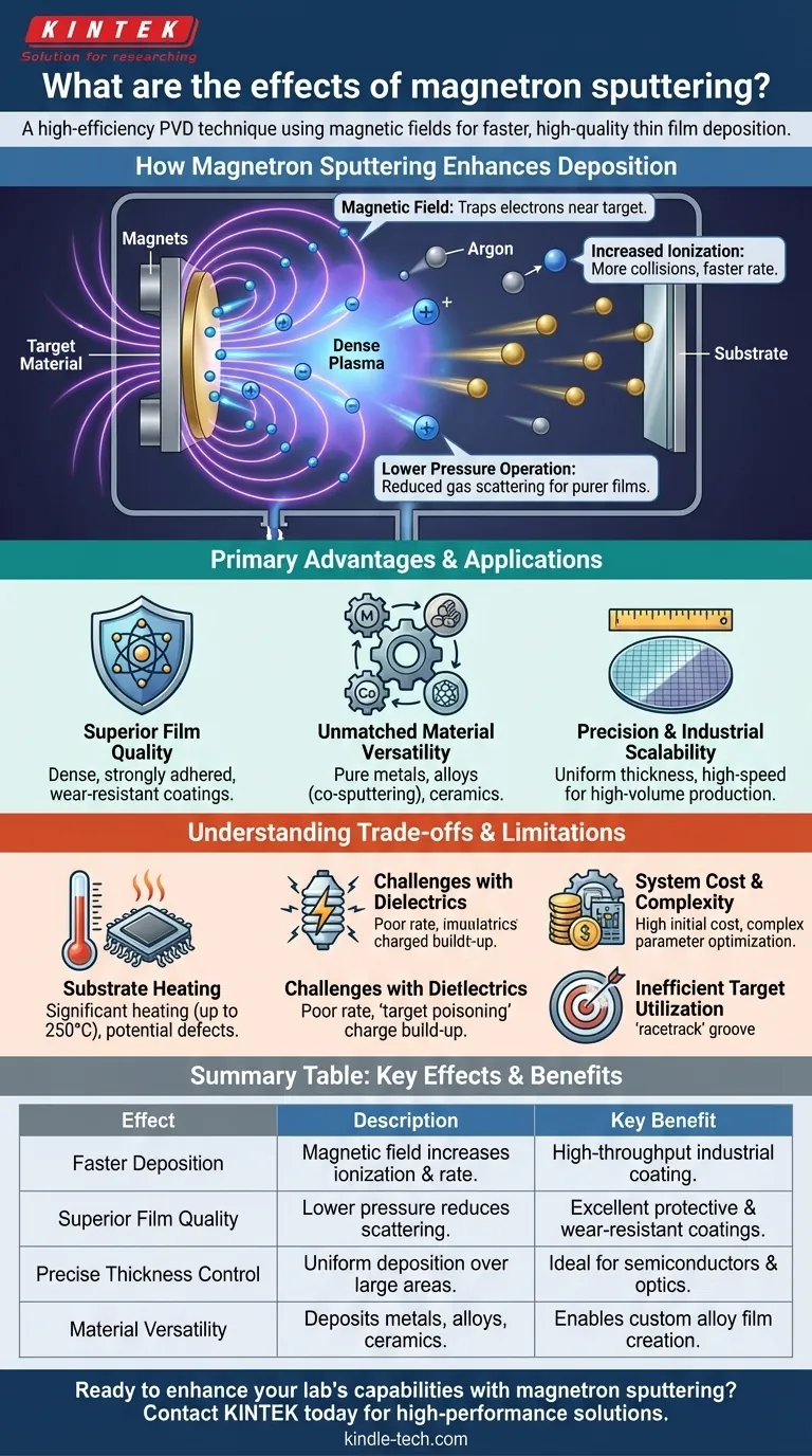
How Magnetron Sputtering Enhances Deposition
To understand the effects of magnetron sputtering, we must first look at its core mechanism. The process refines standard sputtering by adding a powerful magnetic field, which fundamentally changes the plasma environment.
The Role of the Magnetic Field
The key innovation is the strategic placement of magnets behind the sputtering target (the source material). This magnetic field traps electrons in a confined region directly in front of the target surface.
Increased Ionization and Sputtering Rate
These trapped electrons spiral around the magnetic field lines, drastically increasing their path length and the probability of them colliding with neutral gas atoms (typically Argon). This creates a dense, ion-rich plasma precisely where it's needed.
The high concentration of positive gas ions bombards the target material more intensely, ejecting atoms at a much higher rate. This is the primary reason for the technology's speed and efficiency.
Lower Pressure Operation
Because the plasma is so efficiently contained near the target, the process can be run at a much lower gas pressure. This reduces gas-phase scattering of the sputtered atoms, improving the "line of sight" deposition and resulting in purer, denser films.
The Primary Advantages and Applications
The unique mechanism of magnetron sputtering produces several highly desirable outcomes, making it suitable for a vast range of industrial applications.
Superior Film Quality
Magnetron sputtering is known for producing films that are exceptionally dense and exhibit strong adhesion to the substrate. This makes it ideal for protective coatings that must withstand significant wear and environmental stress.
Unmatched Material Versatility
A very wide range of materials can be sputtered, including pure metals, complex alloys, and even some ceramics. By using multiple targets simultaneously (co-sputtering), engineers can create alloy films with highly precise compositions.
Precision and Industrial Scalability
The process allows for uniform and high-precision film thicknesses across large surface areas, which is critical for optics and semiconductors. Its high speed and reliability make it perfectly suited for high-volume, automated industrial production.
Understanding the Trade-offs and Limitations
While powerful, magnetron sputtering is not a universal solution. Understanding its inherent limitations is critical for successful implementation.
Substrate Heating and Potential Defects
The intense ion bombardment is not limited to the target. Energetic particles can also strike the substrate, leading to significant substrate heating, sometimes up to 250°C. This can damage sensitive substrates like plastics or certain electronic components and may introduce structural defects in the growing film.
Challenges with Dielectric Materials
Magnetron sputtering generally has a poor deposition rate for dielectric (electrically insulating) materials. A positive charge can build up on the insulator's surface, repelling the positive ions needed for sputtering, a phenomenon known as "target poisoning."
System Cost and Complexity
The equipment required for magnetron sputtering is mechanically complex and carries a high initial cost. Furthermore, optimizing a process can be time-consuming due to the large number of control parameters that influence the final film properties.
Inefficient Target Utilization
The plasma is often concentrated in a specific ring shape on the target's surface, known as the "racetrack." This leads to uneven erosion and a low utilization rate of the target material, meaning a significant portion of the expensive source material may be wasted.
Making the Right Choice for Your Application
Selecting the right deposition technique depends entirely on your project's specific goals and constraints.
- If your primary focus is high-throughput industrial coating of metals or alloys: Magnetron sputtering is an excellent choice due to its high speed, film quality, and scalability.
- If your primary focus is depositing films onto temperature-sensitive substrates: You must carefully manage the process to mitigate substrate heating or consider alternative, lower-energy deposition methods.
- If your primary focus is depositing thick, high-quality insulating or ceramic films: Standard magnetron sputtering is likely the wrong tool; techniques like RF sputtering or reactive sputtering may be required.
Ultimately, magnetron sputtering is a dominant technology because its effects—speed, quality, and control—align perfectly with the demands of modern, high-volume manufacturing.
Summary Table:
| Effect | Description | Key Benefit |
|---|---|---|
| Faster Deposition | Magnetic field traps electrons, increasing ionization and sputtering rate. | High-throughput coating for industrial production. |
| Superior Film Quality | Lower pressure operation reduces gas scattering, creating dense, well-adhered films. | Excellent for protective and wear-resistant coatings. |
| Precise Thickness Control | Uniform deposition across large areas with high precision. | Ideal for semiconductors, optics, and microelectronics. |
| Material Versatility | Capable of depositing a wide range of metals, alloys, and some ceramics. | Enables creation of custom alloy films via co-sputtering. |
Ready to enhance your lab's capabilities with magnetron sputtering?
At KINTEK, we specialize in providing high-performance lab equipment and consumables tailored to your specific research and production needs. Whether you are developing advanced microelectronics, durable protective coatings, or precision optical components, our expertise in thin-film deposition technology can help you achieve superior results with efficiency and reliability.
Let's discuss how our solutions can benefit your projects. Contact our experts today for a personalized consultation!
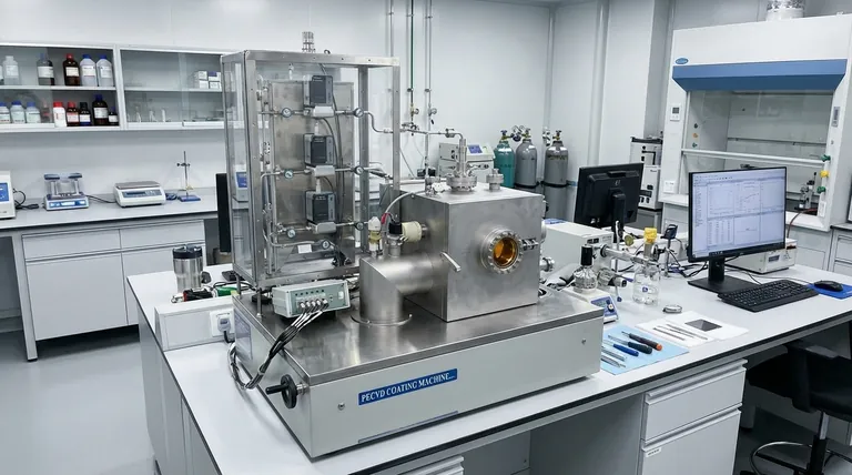
Visual Guide
Related Products
- Spark Plasma Sintering Furnace SPS Furnace
- RF PECVD System Radio Frequency Plasma-Enhanced Chemical Vapor Deposition RF PECVD
People Also Ask
- What technical advantages does a Spark Plasma Sintering (SPS) furnace offer for LZP ceramics? Enhance Ionic Conductivity
- What are the fundamentals of spark plasma sintering process? Unlock Rapid, High-Performance Material Consolidation
- What is the mechanism of SPS process? A Deep Dive into Rapid, Low-Temperature Sintering
- What are the advantages of CAMI/SPS for W-Cu composite preparation? Reduce cycles from hours to seconds.
- What is the process fundamentals of spark plasma sintering? Achieve Rapid, High-Density Material Consolidation

