The formation of a thin film is governed by one of three primary growth modes that dictate its final structure and properties. These are the layer-by-layer mode (Frank-van der Merwe), the island mode (Volmer-Weber), and a hybrid layer-plus-island mode (Stranski-Krastanov). The specific mode is determined by the energetic interplay between the atoms being deposited and the substrate surface.
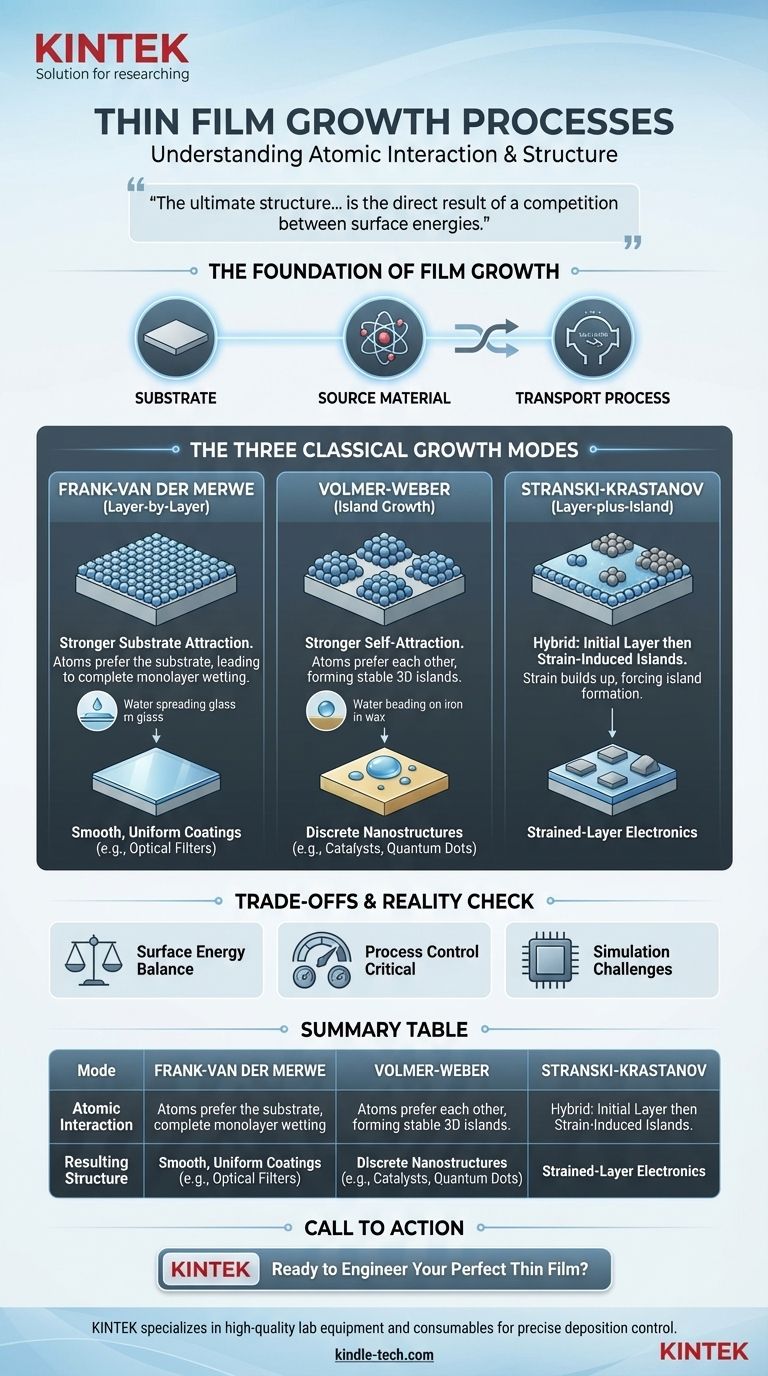
The ultimate structure of a thin film is not random; it is the direct result of a competition between surface energies. Understanding whether depositing atoms prefer to stick to the substrate or to each other is the key to controlling the film's final form and function.
The Foundation of Film Growth
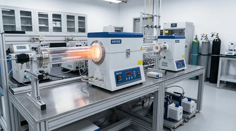
Before a film can grow, three fundamental components must be in place. This process, often occurring in a vacuum chamber, sets the stage for atomic-level assembly.
The Substrate
The substrate is the base material upon which the film is grown. Its surface properties, such as crystal structure and cleanliness, are critical as they provide the template for deposition.
The Source Material
The source, or target material, is the substance that will form the thin film. A deposition technique, such as sputtering, is used to eject atoms from this source.
The Transport Process
These ejected atoms are transported from the source to the substrate. This journey, often through a vacuum or low-pressure gas, concludes when the atoms arrive at the substrate surface with a certain energy.
The Three Classical Growth Modes
Once an atom lands on the substrate, a critical interaction occurs. The balance between the atom's attraction to the substrate versus its attraction to other atoms of the same material dictates how the film will grow.
Frank-van der Merwe (Layer-by-Layer Growth)
This mode occurs when the deposited atoms are more strongly attracted to the substrate than they are to each other. This strong adhesion promotes wetting of the surface.
Each arriving atom prefers to bond to the substrate, leading to the formation of a complete, uniform monolayer before a second layer begins to form. This process repeats, creating an atomically smooth, continuous film. Think of it like water spreading perfectly across a very clean pane of glass.
Volmer-Weber (Island Growth)
This is the opposite scenario, where atoms are more strongly attracted to each other than to the substrate. The cohesive forces within the depositing material are stronger than the adhesive forces to the surface.
Instead of wetting the surface, atoms cluster together to form stable three-dimensional islands. The film grows through the nucleation and eventual merging (coalescence) of these islands. This is analogous to water beading up on a waxy, non-stick surface.
Stranski-Krastanov (Layer-plus-Island Growth)
This is a hybrid mode that combines the other two. Initially, the atoms have a stronger attraction to the substrate, leading to the formation of one or more perfect monolayers, just as in Frank-van der Merwe growth.
However, as these initial layers form, strain builds up within the film due to mismatches in the crystal lattice between the film and the substrate. To relieve this strain energy, the growth mode switches, and the film begins to form 3D islands on top of the initial flat layer.
Understanding the Trade-offs: Theory vs. Reality
While these three modes provide a clear theoretical framework, achieving a desired growth mode in practice presents significant challenges.
The Role of Surface Energy
The choice between growth modes is fundamentally a question of minimizing the total energy of the system. It's a balance between the substrate surface energy, the film's surface energy, and the energy of the interface between them. Modifying the substrate or deposition conditions can shift this balance.
Process Control is Critical
Factors like substrate temperature, deposition rate, and background pressure can influence adatom mobility and sticking coefficients. A process intended for layer-by-layer growth can easily devolve into island formation if conditions are not precisely controlled.
The Challenge of Simulation
Predicting film growth is computationally expensive. While methods like Molecular Dynamics (MD) can model atomic interactions, they are time-consuming and struggle to perfectly capture the complex physics of bond formation and breakage over practical timescales, making experimental validation essential.
Making the Right Choice for Your Goal
Your desired application dictates which growth mode you should target. The film's final properties—be it optical, electrical, or mechanical—are a direct consequence of its nanostructure.
- If your primary focus is a perfectly smooth, uniform coating (e.g., optical filters, protective barriers): You should aim for Frank-van der Merwe growth by choosing a substrate/material combination with strong interfacial adhesion.
- If your primary focus is creating discrete nanostructures (e.g., catalysts, quantum dots): You should leverage Volmer-Weber or Stranski-Krastanov growth to intentionally form controlled 3D islands.
- If your primary focus is a strained film for advanced electronics: You can utilize the initial, highly-strained layers formed during Stranski-Krastanov growth before islanding begins.
By understanding the fundamental principles of atomic interaction, you can move from simply depositing a material to intentionally engineering a thin film with the precise structure needed for your objective.
Summary Table:
| Growth Mode | Atomic Interaction | Resulting Film Structure | Common Applications |
|---|---|---|---|
| Frank-van der Merwe (Layer-by-Layer) | Atoms prefer the substrate | Smooth, uniform, continuous layers | Optical coatings, protective barriers |
| Volmer-Weber (Island Growth) | Atoms prefer each other | 3D islands that coalesce | Catalysts, quantum dots |
| Stranski-Krastanov (Layer-plus-Island) | Initial layer growth, then islanding due to strain | Flat layer with 3D islands on top | Strained-layer electronics |
Ready to engineer the perfect thin film for your research or production? The right growth mode is critical for achieving the desired optical, electrical, or mechanical properties in your final product. At KINTEK, we specialize in providing the high-quality lab equipment and consumables—from sputtering targets to substrates and vacuum components—you need to precisely control your deposition process. Let our experts help you select the ideal tools to achieve your material science goals. Contact our team today to discuss your specific thin film application!
Visual Guide
Related Products
- Tungsten Evaporation Boat for Thin Film Deposition
- Microwave Plasma Chemical Vapor Deposition MPCVD Machine System Reactor for Lab and Diamond Growth
- Cylindrical Resonator MPCVD Machine System Reactor for Microwave Plasma Chemical Vapor Deposition and Lab Diamond Growth
- 915MHz MPCVD Diamond Machine Microwave Plasma Chemical Vapor Deposition System Reactor
- Molybdenum Tungsten Tantalum Evaporation Boat for High Temperature Applications
People Also Ask
- What is the process of thin film deposition? A Guide to PVD, CVD, and Coating Techniques
- What is the method of deposition of thin films? Choose the Right PVD or CVD Technique for Your Lab
- What are the two primary categories of deposition technologies? PVD vs. CVD Explained
- What is the source of evaporation for thin film? Choosing Between Thermal and E-Beam Methods
- What is a thin film evaporator? A Gentle Solution for Heat-Sensitive & Viscous Materials


