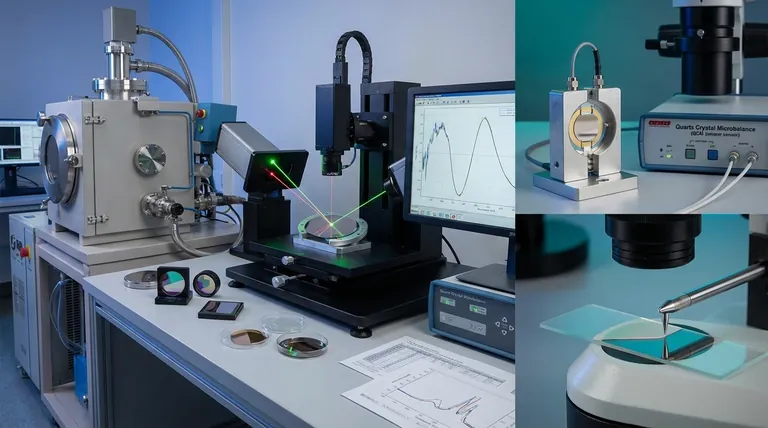
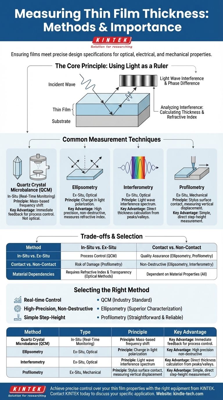
The primary methods for measuring the thickness of thin films are quartz crystal microbalance (QCM) for in-process monitoring, and ellipsometry, interferometry, and profilometry for post-process analysis. These techniques provide critical data, ranging from fractions of a nanometer to several micrometers, ensuring the film meets precise design specifications for its intended application.
Understanding thin film thickness is not just about measuring a physical dimension; it's about controlling the fundamental optical, electrical, and mechanical properties of a final product, from semiconductor chips to advanced optical coatings.
The Core Principle: Using Light as a Ruler
Many of the most common and precise techniques for measuring film thickness are optical. They operate on the principle of light wave interference, a phenomenon that can be used as an incredibly fine-toothed ruler.
How Interference Works
When light strikes a thin film, some of it reflects off the top surface. The rest of the light enters the film, reflects off the bottom surface (the substrate), and travels back out.
These two reflected light waves then combine. Because the second wave traveled a longer path through the film, it is out of phase with the first wave. This phase difference creates an interference pattern of light and dark bands (or peaks and valleys in a spectrum).
Calculating Thickness from the Pattern
By analyzing this interference pattern, specifically the number and position of the peaks and valleys, we can precisely calculate the thickness of the film. This calculation also requires knowing the material's refractive index, as that determines how much the light slows down while traveling through the film.
Common Measurement Techniques Explained
While the principle of interference underpins many methods, different tools are suited for different situations, such as during or after the film has been created.
In-Situ (During Deposition): Quartz Crystal Microbalance (QCM)
A QCM sensor is used inside the deposition chamber to monitor film growth in real-time. It works by measuring a change in the resonant frequency of a quartz crystal as mass (the deposited film) is added to its surface. This is not an optical method but provides immediate feedback for process control.
Optical Methods: Ellipsometry & Interferometry
Ellipsometry is a highly sensitive, non-contact method that measures the change in the polarization of light upon reflection from the thin film. It can determine thickness with sub-nanometer precision and can also provide information on other properties like refractive index.
Interferometry is a more direct application of the interference principle. It analyzes the interference spectrum of reflected light to calculate thickness, relying on the peaks and valleys created by the two reflected light waves.
Mechanical Methods: Profilometry
Profilometry is a contact-based technique. A very fine-tipped stylus is physically dragged across the surface of the film, typically over a pre-made step or edge. By measuring the vertical displacement of the stylus as it moves from the substrate to the film, it directly maps the surface topography and measures the film's height.
Understanding the Trade-offs
No single method is universally superior; the correct choice depends entirely on the application's specific requirements. Choosing a method involves balancing precision, cost, and the need for real-time data.
In-Situ vs. Ex-Situ
In-situ methods like QCM are essential for controlling the deposition process itself, allowing for immediate adjustments. Ex-situ (post-deposition) methods like ellipsometry and profilometry are used for quality assurance and detailed characterization of the final product.
Contact vs. Non-Contact
Contact-based methods like profilometry risk damaging or contaminating a delicate film. Non-contact optical methods like ellipsometry and interferometry are non-destructive, making them ideal for sensitive materials or finished products.
Material Dependencies
Optical methods are dependent on the film being at least partially transparent and require an accurate value for the material's refractive index. If this value is unknown or varies, the thickness calculation will be inaccurate.
Selecting the Right Method for Your Application
Your goal dictates the best tool for the job. Consider what information is most critical for your process.
- If your primary focus is real-time process control: A Quartz Crystal Microbalance (QCM) is the industry standard for monitoring film growth as it happens.
- If your primary focus is high-precision, non-destructive measurement: Ellipsometry is the superior choice for characterizing the thickness and optical properties of the final film with exceptional accuracy.
- If your primary focus is a simple, direct measurement of step height: A stylus profilometer provides a straightforward, reliable measurement for thicker or more robust films where a physical step is available.
Ultimately, accurate measurement is the foundation of creating reliable and high-performance thin film devices.
Summary Table:
| Method | Type | Principle | Key Advantage |
|---|---|---|---|
| Quartz Crystal Microbalance (QCM) | In-Situ | Mass-based frequency shift | Real-time process monitoring |
| Ellipsometry | Ex-Situ, Optical | Change in light polarization | High precision, non-destructive |
| Interferometry | Ex-Situ, Optical | Light wave interference | Direct thickness calculation |
| Profilometry | Ex-Situ, Mechanical | Stylus surface contact | Simple, direct step-height measurement |
Achieve precise control over your thin film properties with the right equipment from KINTEK.
Whether you need real-time monitoring with a Quartz Crystal Microbalance or high-precision characterization with an ellipsometer, selecting the correct measurement tool is critical for the success of your semiconductor, optical coating, or R&D projects. KINTEK specializes in providing high-quality lab equipment and consumables to meet the exacting demands of laboratory professionals.
Let our experts help you choose the perfect solution to ensure your films meet precise design specifications. Contact KINTEK today to discuss your specific application and requirements.
Visual Guide
Related Products
- Small Lab Rubber Calendering Machine
- Electron Beam Evaporation Coating Oxygen-Free Copper Crucible and Evaporation Boat
- Custom PTFE Teflon Parts Manufacturer for PTFE Measuring Cylinder 10/50/100ml
- Thin-Layer Spectral Electrolysis Electrochemical Cell
- Lab Blown Film Extrusion Three Layer Co-Extrusion Film Blowing Machine
People Also Ask
- What is organic thin film? A Guide to Engineered Molecular Layers for Advanced Tech
- What is a calendering machine? Transform Material Surfaces with Precision
- What is the principle of calendering? Enhance Fabric Surface with Heat and Pressure
- What is the process of calendering? A Guide to High-Volume Plastic Film Production
- What finishes are done using calendering technique? Achieve High Gloss, Embossing, and More