At its core, depositing a thin film relies on two primary families of techniques: Physical Vapor Deposition (PVD) and Chemical Vapor Deposition (CVD). These methods, along with more specialized approaches like Atomic Layer Deposition (ALD), are the foundational processes for creating the micro-scale layers essential to modern electronics, optics, and materials science. Each method works by transferring material onto a surface—or "substrate"—but they achieve this goal in fundamentally different ways.
The choice of a deposition method is not arbitrary. It is a strategic decision that balances the material's properties, the desired film characteristics like purity and uniformity, and the specific application's requirements, from semiconductor manufacturing to protective coatings.
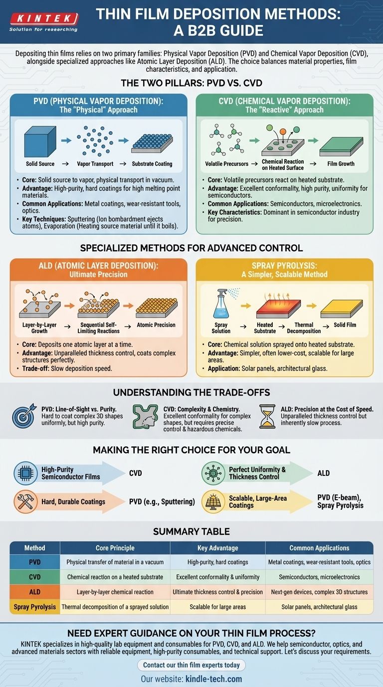
The Two Pillars: PVD vs. CVD
The vast majority of thin film applications are served by two overarching methodologies. Understanding their core difference—one being a physical process and the other a chemical one—is the first step to selecting the right technique.
Physical Vapor Deposition (PVD): The "Physical" Approach
PVD is a process where a solid source material is converted into a vapor and physically transported through a vacuum or low-pressure environment to coat a substrate. Think of it as a highly controlled, atomic-level form of spray painting.
This method is generally preferred for depositing materials with high melting points, such as metals and ceramics, to create hard, wear-resistant coatings.
Key PVD Techniques
Sputtering is a PVD process where atoms are ejected from a solid target material by bombarding it with high-energy ions. These ejected atoms then travel and deposit onto the substrate. Magnetron sputtering is a common variant used for high-quality optical and electrical films.
Evaporation involves heating a source material in a vacuum until it boils. The resulting vapor rises, travels to the cooler substrate, and condenses to form a solid film. E-beam evaporation (using an electron beam) is ideal for solar panels, while thermal evaporation is used for things like OLED displays.
Chemical Vapor Deposition (CVD): The "Reactive" Approach
CVD uses volatile chemical precursors that react or decompose on a heated substrate's surface to produce the desired film. Instead of physically moving solid material, CVD builds the film through a chemical reaction happening directly on the part.
CVD is the dominant method in the semiconductor industry because it produces exceptionally pure, uniform, and conformal films with high precision.
Specialized Methods for Advanced Control
While PVD and CVD cover most applications, certain goals require more specialized processes that offer unique advantages in precision or scalability.
Atomic Layer Deposition (ALD): Ultimate Precision
ALD is a subtype of CVD that deposits material one single atomic layer at a time. It works by exposing the substrate to sequential, self-limiting chemical reactions.
This meticulous process provides unparalleled control over film thickness and can coat extremely complex, high-aspect-ratio structures with perfect uniformity.
Spray Pyrolysis: A Simpler, Scalable Method
This technique involves spraying a chemical solution onto a heated substrate. The heat causes the solution's components to react and thermally decompose, leaving behind a solid film.
It is a simpler, often lower-cost method that can be effective for large-area coatings where absolute atomic-level precision is not the primary concern.
Understanding the Trade-offs
No single method is universally superior. The optimal choice always involves balancing benefits against inherent limitations.
The PVD Compromise: Line-of-Sight vs. Purity
A major limitation of PVD is that it is a line-of-sight process. The vaporized material travels in a straight line, making it difficult to uniformly coat complex 3D shapes with undercuts or hidden surfaces. However, it can produce very high-purity coatings.
The CVD Challenge: Complexity and Chemistry
CVD provides excellent conformality, meaning it can uniformly coat complex shapes. However, the process is more complex, requiring precise control over gas flows, temperature, and pressure. It also relies on precursor chemicals that can be hazardous or expensive.
ALD: Precision at the Cost of Speed
The primary trade-off for ALD is speed. Building a film one atomic layer at a time is an inherently slow process. It is chosen only when the absolute need for thickness control and conformality outweighs the need for high throughput.
Making the Right Choice for Your Goal
Your choice of method depends entirely on the specific outcome you need to achieve for your project.
- If your primary focus is manufacturing high-purity films for semiconductors: CVD is the industry standard due to its excellent uniformity and ability to coat complex wafer topographies.
- If your primary focus is depositing hard, durable coatings on tools or simple surfaces: PVD methods like sputtering are often the most direct and effective approach.
- If your primary focus is creating perfectly uniform films with absolute thickness control for next-gen devices: ALD offers unparalleled precision, though at a slower deposition rate.
- If your primary focus is scalable, large-area coatings for applications like solar panels or architectural glass: Specific PVD techniques like e-beam evaporation or simpler methods like spray pyrolysis are highly suitable.
Understanding these fundamental principles empowers you to select not just a method, but the correct method for your specific engineering goal.
Summary Table:
| Method | Core Principle | Key Advantage | Common Applications |
|---|---|---|---|
| PVD (Physical Vapor Deposition) | Physical transfer of material in a vacuum | High-purity, hard coatings | Metal coatings, wear-resistant tools, optics |
| CVD (Chemical Vapor Deposition) | Chemical reaction on a heated substrate | Excellent conformality & uniformity | Semiconductors, microelectronics |
| ALD (Atomic Layer Deposition) | Layer-by-layer chemical reaction | Ultimate thickness control & precision | Next-gen devices, complex 3D structures |
| Spray Pyrolysis | Thermal decomposition of a sprayed solution | Scalable for large areas | Solar panels, architectural glass |
Need expert guidance on your thin film process?
Choosing the right deposition method is critical for your project's success. KINTEK specializes in providing high-quality lab equipment and consumables for all your thin film research and development needs. Whether you are working with PVD, CVD, or ALD, our expertise can help you achieve superior film quality, consistency, and performance.
We help our customers in the semiconductor, optics, and advanced materials sectors by:
- Providing reliable equipment for precise and repeatable deposition.
- Supplying high-purity consumables like targets and precursors to ensure optimal results.
- Offering technical support to optimize your process parameters and overcome challenges.
Let's discuss your specific application requirements. Contact our thin film experts today to find the perfect solution for your laboratory.
Visual Guide
Related Products
- Aluminized Ceramic Evaporation Boat for Thin Film Deposition
- Tungsten Evaporation Boat for Thin Film Deposition
- Electron Beam Evaporation Coating Oxygen-Free Copper Crucible and Evaporation Boat
- Molybdenum Tungsten Tantalum Evaporation Boat for High Temperature Applications
- Vacuum Hot Press Furnace Machine for Lamination and Heating
People Also Ask
- What are the alternatives to sputtering? Choose the Right Thin Film Deposition Method
- What is thin film deposition? Unlock Advanced Surface Engineering for Your Materials
- Why is an alumina boat selected for catalyst precursors? Ensure Sample Purity at 1000 °C
- What are thin films deposited by evaporation? A Guide to High-Purity Coating
- What is the source of evaporation for thin film? Choosing Between Thermal and E-Beam Methods


