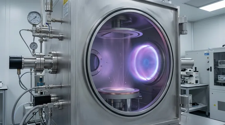
In essence, the sputtering process is a physical vapor deposition technique that operates in a high vacuum. It uses energetic ions from a plasma to bombard a source material, known as the target, which dislodges atoms. These liberated atoms then travel through the vacuum chamber and deposit onto a substrate, building a new, high-purity thin film layer by layer.
Sputtering is not a chemical reaction but a physical process of momentum transfer, akin to a microscopic game of billiards. By creating a high-vacuum environment and energizing a plasma, we can precisely control the bombardment of a target to build a new material, atom by atom.
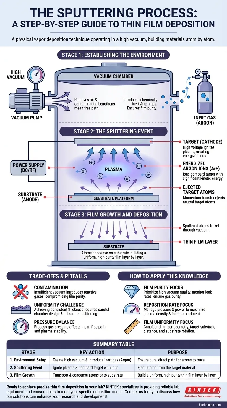
Stage 1: Establishing the Environment
The success of the entire sputtering process depends on meticulously preparing the chamber environment before any deposition occurs.
Creating the High Vacuum
The first and most critical step is creating a vacuum inside the process chamber using a vacuum pump. Air and other contaminants are removed.
This vacuum is non-negotiable because it dramatically lengthens the mean free path of particles. This ensures that atoms sputtered from the target can travel directly to the substrate without colliding with unwanted air or water molecules.
Introducing the Process Gas
Once a sufficient vacuum is achieved, a controlled amount of a high-purity, inert gas is introduced into the chamber.
Argon is the most common choice. Because it is chemically inert, it will not react with the target material, ensuring the deposited film is composed purely of the target's atoms.
Stage 2: The Sputtering Event
This stage is the core of the process, where the physical mechanism of sputtering takes place. It is a rapid, self-sustaining chain of events.
Igniting the Plasma
A high voltage is applied to the target material, which acts as a cathode (negative electrode). This powerful electric field energizes the inert gas atoms.
This energy strips electrons from the gas atoms, creating a mixture of free electrons and positively charged ions. This energized, ionized gas is known as a plasma.
Ion Bombardment
The negatively charged target violently attracts the newly formed, positively charged argon ions from the plasma.
These ions accelerate toward the target, striking its surface with significant kinetic energy. This is the "bombardment" phase.
Ejecting Target Atoms
When an energetic ion collides with the target, it transfers its momentum to the target's atoms. If the energy transfer is sufficient, it will knock one or more atoms completely free from the target's surface.
These ejected, neutral atoms are the material that will ultimately form the thin film.
Stage 3: Film Growth and Deposition
The final stage involves the journey of the ejected atoms and their accumulation on the substrate.
Transport Through the Vacuum
The sputtered atoms travel in a straight line from the target through the vacuum-filled chamber. The quality of the vacuum is critical here to prevent these atoms from colliding with other particles, which would scatter them and result in a non-uniform film.
Condensation on the Substrate
When the sputtered atoms reach the surface of the substrate (the material being coated), they condense and stick.
Over time, this continuous bombardment of atoms builds up on the substrate, layer by layer, forming a dense and uniform thin film.
Understanding the Trade-offs and Pitfalls
While powerful, sputtering is a process of precision where small deviations can have significant consequences.
The Constant Enemy: Contamination
An insufficient vacuum is the primary source of failure. If reactive gases like oxygen or water vapor remain in the chamber, they can react with the sputtered atoms and become incorporated into the growing film, compromising its purity and performance.
The Challenge of Uniformity
Achieving a perfectly uniform film thickness across a large substrate is challenging. It requires careful design of the chamber, the positioning of the substrate relative to the target, and sometimes substrate rotation to average out any inconsistencies in the flux of sputtered atoms.
The Pressure Balance
The pressure of the process gas (e.g., argon) is a critical variable. Too high a pressure reduces the mean free path, causing sputtered atoms to scatter. Too low a pressure can make it difficult to sustain a stable plasma, leading to a very low deposition rate.
How to Apply This Knowledge
Understanding these fundamental steps transforms sputtering from a "black box" into a predictable engineering tool.
- If your primary focus is film purity and quality: Your first priority must be the quality of the vacuum. Monitor leak rates and ensure the purity of the process gas.
- If your primary focus is deposition rate: You must manage the relationship between process gas pressure and applied power to maximize plasma density and, therefore, the ion bombardment rate.
- If your primary focus is film uniformity: You must consider the geometry of the chamber, the target-to-substrate distance, and the potential need for substrate rotation.
By mastering these core stages, you gain direct control over the properties and quality of the final material.
Summary Table:
| Stage | Key Action | Purpose |
|---|---|---|
| 1. Environment Setup | Create high vacuum & introduce inert gas (Argon) | Ensure pure, direct path for atoms to travel |
| 2. Sputtering Event | Ignite plasma & bombard target with ions | Eject atoms from the target material |
| 3. Film Growth | Transport & condense atoms onto substrate | Build a uniform, high-purity thin film layer by layer |
Ready to achieve precise thin film deposition in your lab? The sputtering process is key to creating high-quality coatings for semiconductors, optics, and research applications. KINTEK specializes in providing reliable lab equipment and consumables to meet your specific deposition needs.
Contact us today to discuss how our solutions can enhance your research and development!
Visual Guide
Related Products
- Spark Plasma Sintering Furnace SPS Furnace
- Vacuum Induction Melting Spinning System Arc Melting Furnace
- Chemical Vapor Deposition CVD Equipment System Chamber Slide PECVD Tube Furnace with Liquid Gasifier PECVD Machine
- Customer Made Versatile CVD Tube Furnace Chemical Vapor Deposition Chamber System Equipment
People Also Ask
- What are the advantages of CAMI/SPS for W-Cu composite preparation? Reduce cycles from hours to seconds.
- What is the process fundamentals of spark plasma sintering? Achieve Rapid, High-Density Material Consolidation
- What are the fundamentals of spark plasma sintering process? Unlock Rapid, High-Performance Material Consolidation
- What is the pressure for spark plasma sintering? A Guide to Optimizing SPS Parameters
- What technical advantages does a Spark Plasma Sintering (SPS) furnace offer for LZP ceramics? Enhance Ionic Conductivity


