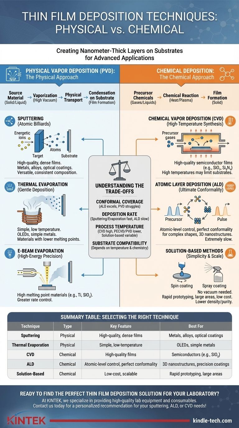
At its core, thin film deposition involves applying a material layer, often mere nanometers thick, onto a substrate. These techniques are broadly divided into two families: Physical Vapor Deposition (PVD), where a material is physically transferred, and Chemical Deposition, where a new material is formed on the substrate through chemical reactions. Key examples include sputtering and evaporation (PVD), and Chemical Vapor Deposition (CVD) and Atomic Layer Deposition (ALD) for chemical methods.
The central challenge is not simply knowing the list of deposition techniques, but understanding that each method represents a distinct trade-off. Your choice will always be a balance between film quality, deposition speed, material compatibility, and process cost.
The Two Pillars of Deposition: Physical vs. Chemical
The fundamental distinction between deposition techniques lies in how the film material arrives at the substrate surface. This difference dictates the properties of the film and the complexity of the process.
The Physical Approach: Moving Atoms
In Physical Vapor Deposition (PVD), a solid or liquid source material is converted into a vapor and physically transported to the substrate, where it condenses to form the film. This process is almost always conducted in a high-vacuum environment to ensure purity.
The Chemical Approach: Building with Molecules
In Chemical Deposition, precursor chemicals (gases or liquids) are introduced to the substrate. A chemical reaction is then induced—often by heat or plasma—causing the precursors to decompose and form a new, solid film on the surface.
An Overview of Key Physical Techniques (PVD)
PVD methods are workhorses for depositing metals, alloys, and many ceramic compounds. They are valued for creating dense, high-purity films.
Sputtering: Atomic Billiards
Sputtering uses energetic ions (typically argon) to bombard a solid "target" of the desired material. This bombardment ejects, or "sputters," atoms from the target, which then travel and deposit onto the substrate. It is highly versatile and excellent for depositing alloys and compounds with consistent composition.
Thermal Evaporation: Gentle Deposition
This is one of the simplest PVD methods. The source material is placed in a crucible and heated in a vacuum until it evaporates. The vapor rises, travels in a straight line, and condenses on the cooler substrate. It is well-suited for materials with lower melting points, such as aluminum or organic compounds for OLEDs.
E-Beam Evaporation: High-Energy Precision
Electron-Beam (E-Beam) Evaporation is a more advanced form of thermal evaporation. It uses a high-energy beam of electrons to heat the source material. This allows for the deposition of materials with very high melting points, like titanium or silicon dioxide, and offers greater control over the deposition rate.
An Overview of Key Chemical Techniques
Chemical deposition methods are essential for creating highly uniform and conformal films, which is critical in semiconductor manufacturing and for coating complex shapes.
Chemical Vapor Deposition (CVD): High-Temperature Synthesis
In CVD, precursor gases flow over a heated substrate. The high temperature triggers a chemical reaction, depositing a solid film. CVD is a cornerstone of the semiconductor industry for producing high-quality silicon dioxide and silicon nitride films, but its high-temperature requirement can limit the types of substrates that can be used.
Atomic Layer Deposition (ALD): Ultimate Conformality
ALD is a unique subclass of CVD that builds films one single atomic layer at a time. It uses a sequence of self-limiting chemical reactions. This process provides unparalleled control over film thickness and can perfectly coat extremely complex, high-aspect-ratio structures. The trade-off is that it is significantly slower than other methods.
Solution-Based Methods: Simplicity and Scale
Techniques like spin coating, dip coating, and spray pyrolysis are chemical methods that do not require a vacuum. A liquid chemical precursor (a sol-gel) is applied to the substrate, followed by heating to drive reactions and solidify the film. These methods are simple, low-cost, and scalable but generally produce films of lower density and purity than vapor-based techniques.
Understanding the Trade-offs
Choosing the right technique requires a clear understanding of your project's priorities. No single method is universally superior.
Conformal Coverage: Coating Complex Shapes
The ability to uniformly coat a non-flat surface is called conformality. ALD offers near-perfect conformality, making it ideal for 3D nanostructures. In contrast, PVD methods are "line-of-sight" processes and struggle to coat sidewalls or complex topographies.
Deposition Rate vs. Film Control
There is a direct trade-off between speed and precision. Sputtering and evaporation are relatively fast, depositing many nanometers per minute. ALD, on the other hand, is extremely slow, depositing fractions of a nanometer per minute, but offers angstrom-level control.
Process Temperature and Substrate Compatibility
High-temperature processes like conventional CVD can damage sensitive substrates like plastics or certain electronic components. PVD techniques and specialized methods like Plasma-Enhanced CVD (PECVD) can operate at much lower temperatures, expanding the range of compatible substrates.
Selecting the Right Technique for Your Application
Your choice must be driven by your primary objective.
- If your primary focus is ultimate precision and coating complex 3D structures: ALD is the unrivaled choice due to its atomic-level control and perfect conformality.
- If your primary focus is depositing high-quality metals or optical coatings at high speed: Sputtering (PVD) offers an excellent balance of film quality and industrial throughput.
- If your primary focus is depositing sensitive organic materials for OLEDs or simple metals for electronics: Thermal Evaporation (PVD) is a cost-effective and gentle method.
- If your primary focus is rapid prototyping or coating large areas at low cost without vacuum: Solution-based methods like spin coating or spray pyrolysis are the most practical options.
By aligning the unique strengths and weaknesses of each technique with your end goal, you can confidently select the deposition method that will lead to a successful outcome.
Summary Table:
| Technique | Type | Key Feature | Best For |
|---|---|---|---|
| Sputtering (PVD) | Physical | High-quality, dense films | Metals, alloys, optical coatings |
| Thermal Evaporation (PVD) | Physical | Simple, low-temperature | OLEDs, simple metals |
| CVD | Chemical | High-quality films | Semiconductors (e.g., SiO₂) |
| ALD | Chemical | Atomic-level control, perfect conformality | 3D nanostructures, precision coatings |
| Solution-Based (e.g., Spin Coating) | Chemical | Low-cost, scalable | Rapid prototyping, large areas |
Ready to find the perfect thin film deposition solution for your laboratory? The right technique is critical for achieving the film quality, uniformity, and performance your research demands. At KINTEK, we specialize in providing high-quality lab equipment and consumables for all your deposition needs. Our experts can help you select the ideal PVD or chemical deposition system—whether it's a sputtering tool for metal coatings or an ALD reactor for ultra-thin films—ensuring your project's success. Contact us today to discuss your specific application and receive a personalized recommendation!
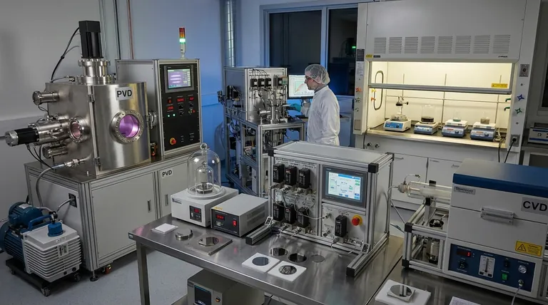
Visual Guide
Related Products
- Aluminized Ceramic Evaporation Boat for Thin Film Deposition
- Tungsten Evaporation Boat for Thin Film Deposition
- Electron Beam Evaporation Coating Oxygen-Free Copper Crucible and Evaporation Boat
- Molybdenum Tungsten Tantalum Evaporation Boat for High Temperature Applications
- Vacuum Hot Press Furnace Machine for Lamination and Heating
People Also Ask
- What are the applications of thin films deposition? Unlock New Possibilities for Your Materials
- What is the chemical method for thin film deposition? Build Films from the Molecular Level Up
- Why is an alumina boat selected for catalyst precursors? Ensure Sample Purity at 1000 °C
- What is thin film deposition? Unlock Advanced Surface Engineering for Your Materials
- Why are high-purity ceramic boats used for lignin activation? Ensure Purity & Thermal Stability


