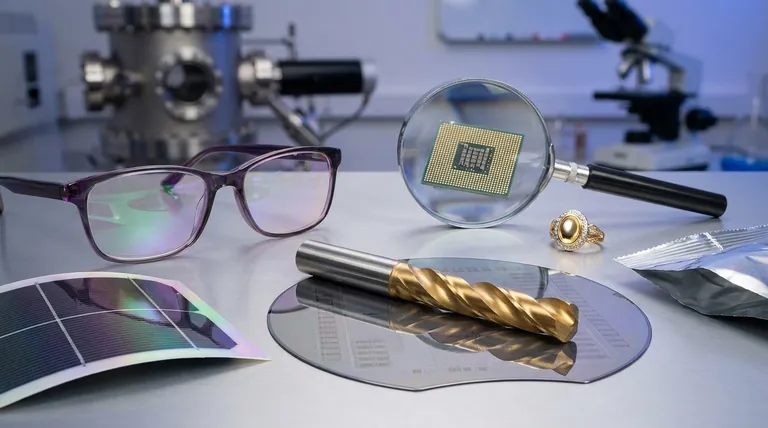
At their core, thin films are used to impart new properties to the surface of a material. These engineered layers, often just nanometers to micrometers thick, can make a surface protective, optically active, electrically conductive, or simply decorative. Their applications are vast, ranging from the anti-reflective coatings on your eyeglasses to the complex circuitry inside your smartphone and the panels of a solar farm.
The fundamental purpose of a thin film is not to exist on its own, but to fundamentally change the behavior of the bulk material it coats. It allows engineers to select a substrate for its structural properties (like glass for transparency or steel for strength) and then add a completely different set of surface properties (like conductivity or corrosion resistance).
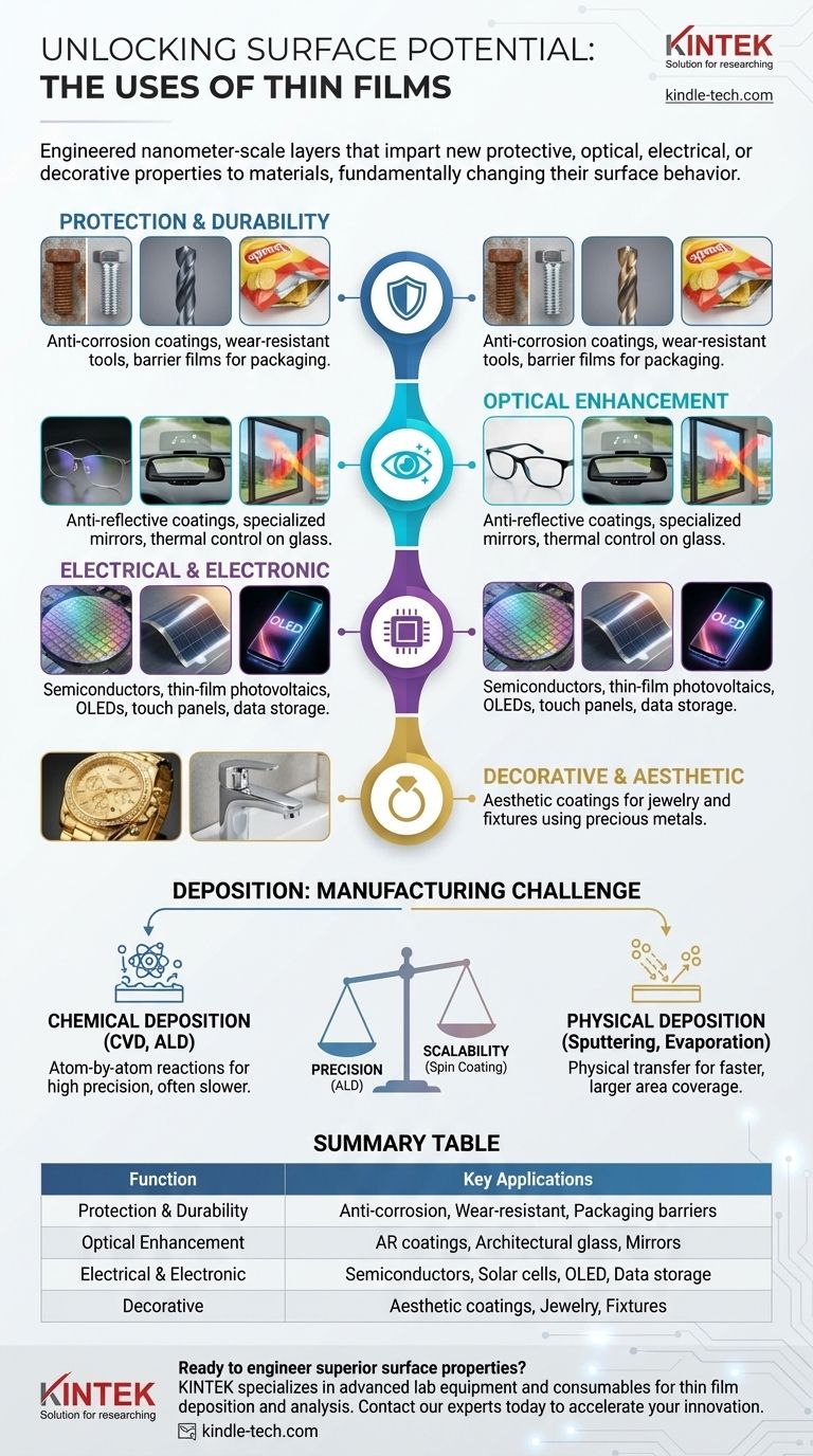
The Functional Roles of Thin Films
The versatility of thin films comes from their ability to perform a specific function by precisely controlling material properties at a microscopic scale. We can categorize their uses by the primary function they serve.
For Protection and Durability
A thin film can act as a physical barrier, isolating the underlying material (the substrate) from its environment.
This is one of the most common and commercially important uses. A film of a corrosion-resistant material can be deposited onto a cheaper or stronger metal, dramatically extending the component's life.
Similarly, extremely hard materials can be applied as thin films onto cutting tools, drills, and machine parts. This significantly reduces wear and friction, improving performance and longevity.
Even the metallic lining inside a bag of chips is a thin film. It acts as a barrier to oxygen and moisture, preserving the freshness of the food inside.
For Optical Enhancement
Thin films are critical for manipulating light. By controlling the thickness and refractive index of one or more layers, we can dictate how light reflects, transmits, or is absorbed.
Antireflective coatings on ophthalmic lenses, camera lenses, and solar cells use destructive interference to minimize reflections and maximize light transmission.
Conversely, highly reflective films are used to create mirrors, from simple household mirrors to the specialized reflectors in lamps and automotive head-up displays (HUDs).
In architecture, thin films on glass can reflect infrared radiation (heat) while allowing visible light to pass through. This provides thermal insulation, keeping buildings cooler in the summer and warmer in the winter.
For Electrical and Electronic Functionality
Modern electronics would be impossible without thin films. The entire semiconductor industry is built on depositing and etching complex stacks of conductive, insulating, and semiconducting thin films to create integrated circuits.
Thin-film photovoltaic cells use layers of specific materials that convert light energy directly into electrical power. This technology is key to flexible and lightweight solar panels.
Devices like Organic Light Emitting Diodes (OLEDs) and touch panels rely on transparent conductive films. These layers can carry an electrical current without obstructing the light from the display.
Thin films are also used in data storage, from magnetic layers on hard disk platters to the materials used in advanced computer memory.
For Decorative and Aesthetic Purposes
Finally, thin films can be used for purely aesthetic reasons. A very thin layer of gold or other precious metals can be applied to jewelry or bathroom fittings, providing a high-end appearance without the cost and weight of a solid object.
Understanding the Manufacturing Challenge: Deposition
A thin film's properties are inseparable from how it is made. The choice of deposition method is a critical engineering decision that dictates the film's quality, cost, and suitability for an application.
The Two Major Pathways
Deposition techniques are broadly divided into two families.
Chemical Deposition methods, like Chemical Vapor Deposition (CVD) and Atomic Layer Deposition (ALD), use chemical reactions at the substrate's surface to build the film layer by layer.
Physical Deposition methods, like sputtering and thermal evaporation, use physical means (e.g., vaporizing or bombarding a source material) to transfer atoms onto the substrate.
The Trade-off: Precision vs. Scalability
No single deposition method is best for everything. There is an inherent trade-off between atomic-level precision and manufacturing speed or cost.
Methods like Atomic Layer Deposition (ALD) offer unparalleled control, allowing for the creation of perfectly uniform films one atomic layer at a time. This is essential for advanced microchips but can be slow and expensive.
In contrast, techniques like spin coating or dip coating are much faster and cheaper for covering large areas, making them suitable for applications like flexible displays or certain optical coatings, but they offer less fine-grained control.
Material and Substrate Compatibility
The choice of method also depends on the materials involved. Some materials can be easily evaporated (physical), while others are better formed through chemical reactions. The substrate itself also plays a role; its temperature tolerance and surface chemistry can limit which deposition processes are viable.
How to Apply This to Your Goal
The right thin film application depends entirely on the problem you are trying to solve.
- If your primary focus is industrial durability and efficiency: Your key takeaway is using hard, wear-resistant, and anti-corrosive coatings to extend the life of tools and machinery.
- If your primary focus is advanced electronics: The focus is on the precise, layered deposition of semiconductor, conductive, and insulating films to build complex microelectronic devices, displays, and sensors.
- If your primary focus is energy and sustainability: The key applications are thin-film photovoltaics for solar power generation and thermal control coatings on architectural glass for energy efficiency.
- If your primary focus is optics: Your goal is to use single or multiple layers of transparent materials to control reflection and transmission for lenses, mirrors, and filters.
Ultimately, thin films empower us to engineer the surface of an object independently of its bulk, unlocking a world of technological possibility.
Summary Table:
| Function | Key Applications |
|---|---|
| Protection & Durability | Anti-corrosion coatings, wear-resistant tool coatings, barrier films for packaging |
| Optical Enhancement | Anti-reflective coatings for lenses, architectural glass for thermal control, mirrors |
| Electrical & Electronic | Semiconductor circuits, thin-film solar cells, OLED displays, touch panels, data storage |
| Decorative | Aesthetic coatings for jewelry and fixtures using precious metals |
Ready to engineer superior surface properties for your materials?
KINTEK specializes in providing advanced lab equipment and consumables for thin film deposition and analysis. Whether your focus is on enhancing durability for industrial tools, developing next-generation electronics, or creating efficient energy solutions, our expertise can help you achieve precise and reliable results.
Contact our experts today to discuss how our solutions can meet your specific laboratory needs and accelerate your innovation.
Visual Guide
Related Products
- Aluminized Ceramic Evaporation Boat for Thin Film Deposition
- Tungsten Evaporation Boat for Thin Film Deposition
- Electron Beam Evaporation Coating Oxygen-Free Copper Crucible and Evaporation Boat
- Molybdenum Tungsten Tantalum Evaporation Boat for High Temperature Applications
- Aluminum-Plastic Flexible Packaging Film for Lithium Battery Packaging
People Also Ask
- What are the alternatives to sputtering? Choose the Right Thin Film Deposition Method
- What are the applications of thin films deposition? Unlock New Possibilities for Your Materials
- What are thin films deposited by evaporation? A Guide to High-Purity Coating
- Why are high-purity ceramic boats used for lignin activation? Ensure Purity & Thermal Stability
- Why is an alumina boat selected for catalyst precursors? Ensure Sample Purity at 1000 °C


