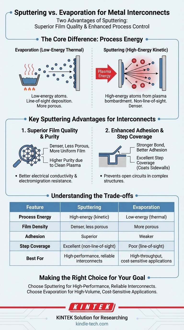
Two primary advantages of sputtering over evaporation for creating metal interconnect systems are superior film quality and enhanced process control. Sputtering utilizes a high-energy plasma environment to produce denser, purer, and more uniform films with better adhesion, which is critical for the reliability of modern integrated circuits.
The core difference lies in the energy of the deposition process. Evaporation is a low-energy thermal process driven by heat, while sputtering is a high-energy kinetic process driven by plasma bombardment, granting it superior control over the final film's properties.
The Physical Process: Why Energy Matters
To understand the advantages, we must first look at the fundamental difference between how these two methods deposit atoms onto a substrate.
Evaporation: A Line-of-Sight Thermal Method
Evaporation involves heating a source material in a vacuum chamber until it vaporizes. The gaseous atoms then travel in a straight line and condense on the cooler substrate, forming a thin film.
This process is relatively simple and fast, but the low energy of the evaporated atoms can result in a more porous film with weaker adhesion.
Sputtering: A High-Energy Kinetic Method
Sputtering takes place in a plasma environment. High-energy ions are accelerated to strike a "target" made of the desired material.
This bombardment ejects, or "sputters," atoms from the target with significant kinetic energy. These high-energy atoms then deposit onto the substrate, creating a fundamentally different type of film.
Key Sputtering Advantages for Interconnects
The high-energy nature of the sputtering process directly translates into tangible benefits for creating robust and reliable metal interconnects.
Advantage 1: Superior Film Quality and Purity
Sputtered atoms arrive at the substrate with much higher energy than evaporated atoms. This energy allows them to move around on the surface momentarily, finding optimal positions in the film's crystal lattice.
The result is a denser, less porous, and more uniform film. This density is critical for interconnects, as it leads to better electrical conductivity and resistance to electromigration, a common failure mechanism. The plasma environment also provides a cleaner deposition, leading to higher purity.
Advantage 2: Enhanced Adhesion and Step Coverage
Adhesion is paramount for interconnects, which must reliably stick to the underlying dielectric layers. The high kinetic energy of sputtered atoms effectively embeds them into the substrate surface, creating a much stronger bond than the simple condensation of evaporation.
Furthermore, sputtering provides better step coverage. Because atoms are ejected from the target in various directions, they can coat the sides and bottoms of trenches and vias more effectively than the line-of-sight deposition from evaporation, preventing open circuits.
Understanding the Trade-offs
Choosing a deposition method always involves balancing competing factors. While sputtering offers superior quality, it is not always the optimal choice.
Cost and Complexity
Sputtering systems are generally more complex and expensive to purchase and maintain. They require sophisticated power supplies for the plasma, high-quality vacuum systems, and argon gas handling. Evaporation systems are comparatively simpler and more cost-effective.
Deposition Rate
For many materials, thermal evaporation offers a significantly higher deposition rate than sputtering. This makes it more suitable for applications where high throughput and low cost are more important than the absolute highest film quality.
Material and Substrate Compatibility
The high-energy plasma in sputtering can sometimes cause damage to sensitive substrates. In contrast, the lower-energy nature of evaporation is gentler, making it a better choice for certain organic or delicate materials.
Making the Right Choice for Your Goal
Your application's specific requirements for performance, cost, and throughput will determine the best method.
- If your primary focus is high-performance, reliable interconnects: Sputtering is the superior choice for its ability to produce dense, pure films with excellent adhesion and step coverage.
- If your primary focus is high-volume production for less critical applications: Evaporation offers a compelling advantage in speed and cost-effectiveness.
Ultimately, the decision hinges on whether your priority is the uncompromising film quality of sputtering or the economic efficiency of evaporation.
Summary Table:
| Feature | Sputtering | Evaporation |
|---|---|---|
| Process Energy | High-energy (kinetic) | Low-energy (thermal) |
| Film Density | Denser, less porous | More porous |
| Adhesion | Superior | Weaker |
| Step Coverage | Excellent (non-line-of-sight) | Poor (line-of-sight) |
| Best For | High-performance, reliable interconnects | High-throughput, cost-sensitive applications |
Need to deposit high-quality metal films for your interconnects? KINTEK specializes in advanced lab equipment, including sputtering and evaporation systems, to help you achieve the precise film properties your research or production demands. Our experts can help you select the right deposition technology for superior adhesion, density, and reliability. Contact our team today to discuss your specific application and find the optimal solution!
Visual Guide
Related Products
- Spark Plasma Sintering Furnace SPS Furnace
- Vacuum Induction Melting Spinning System Arc Melting Furnace
- Chemical Vapor Deposition CVD Equipment System Chamber Slide PECVD Tube Furnace with Liquid Gasifier PECVD Machine
- Customer Made Versatile CVD Tube Furnace Chemical Vapor Deposition Chamber System Equipment
- Vacuum Cold Mounting Machine for Sample Preparation
People Also Ask
- What is the theory of spark plasma sintering? A Guide to Rapid, Low-Temperature Densification
- What is the process fundamentals of spark plasma sintering? Achieve Rapid, High-Density Material Consolidation
- What is SPS sintering method? A Guide to High-Speed, High-Performance Material Fabrication
- What technical advantages does a Spark Plasma Sintering (SPS) furnace offer for LZP ceramics? Enhance Ionic Conductivity
- What are the advantages of CAMI/SPS for W-Cu composite preparation? Reduce cycles from hours to seconds.


