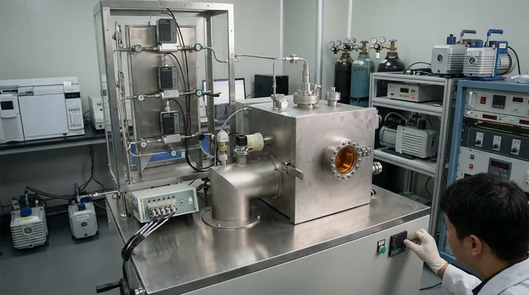
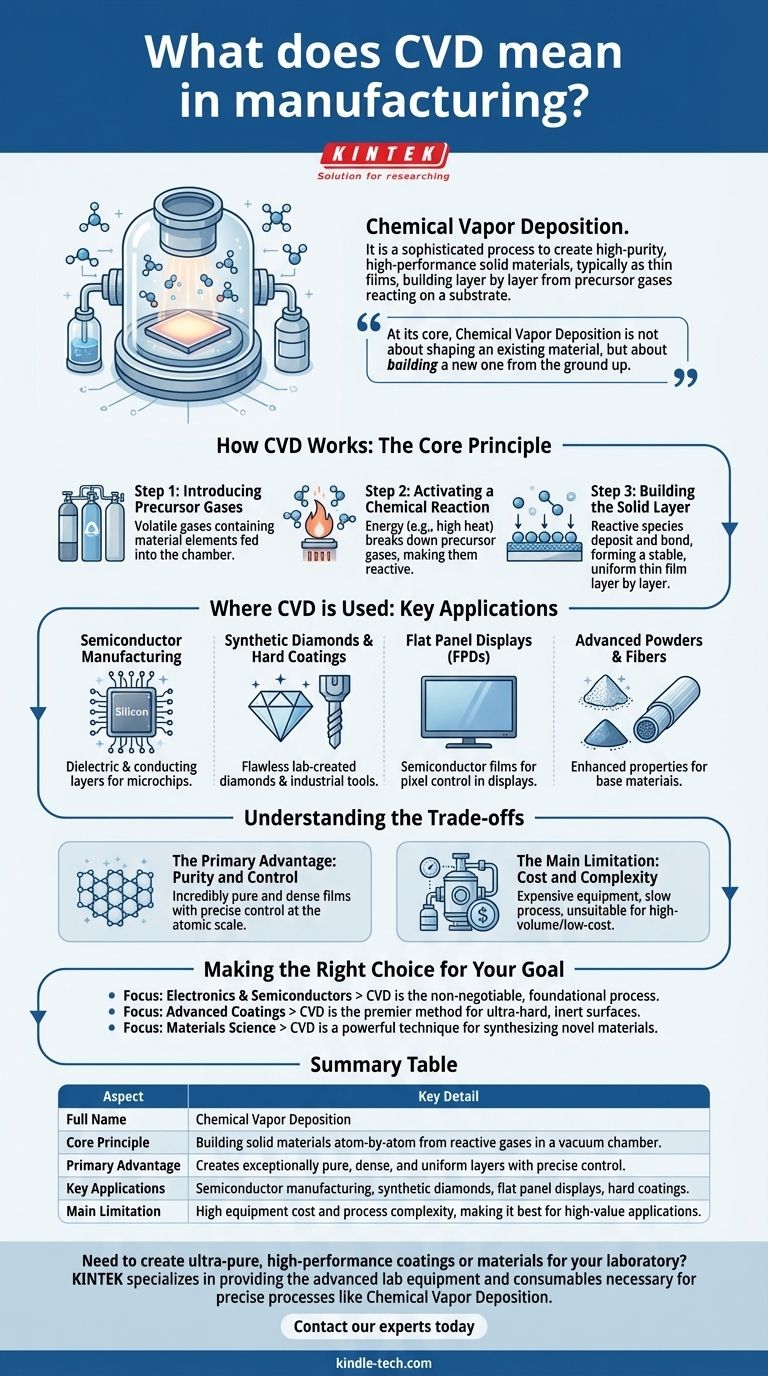
In manufacturing, CVD stands for Chemical Vapor Deposition. It is a sophisticated process used to create high-purity, high-performance solid materials, typically in the form of thin films or coatings. The method involves introducing precursor gases into a chamber, which then react and decompose to deposit a solid layer onto the surface of a substrate, building the material one layer of atoms or molecules at a time.
At its core, Chemical Vapor Deposition is not about shaping an existing material, but about building a new one from the ground up. It is the go-to technique when a manufacturer needs to create an exceptionally pure, dense, and uniform layer with precisely controlled properties.
How CVD Works: The Core Principle
CVD is a process of controlled chemical reaction and deposition. It occurs within a sealed vacuum chamber to ensure no contaminants interfere with the process.
Step 1: Introducing Precursor Gases
The process begins by feeding one or more volatile gases, known as precursors, into the reaction chamber. These gases contain the chemical elements that will make up the final solid material. The object to be coated, called the substrate, is also placed inside this chamber.
Step 2: Activating a Chemical Reaction
Energy, typically in the form of high heat, is applied to the chamber. This energy breaks down the precursor gases, causing them to become chemically reactive. Think of it as "unlocking" the atoms held within the gas molecules.
Step 3: Building the Solid Layer
The reactive chemical species then deposit onto the surface of the substrate. As they land, they form strong chemical bonds with the substrate and with each other, creating a stable, solid, and exceptionally uniform thin film. This process continues, building the film layer by layer.
Where CVD is Used: Key Applications
Because of its precision, CVD is a critical technology in industries that rely on high-performance materials.
Semiconductor Manufacturing
This is the most significant application of CVD. It is used to deposit the various insulating (dielectric) and conducting layers that form the microscopic transistors and circuits on a silicon wafer, the foundation of every computer chip.
Synthetic Diamonds and Hard Coatings
CVD is a primary method for growing lab-created diamonds. The process allows for the creation of flawless, high-purity diamond films that can be used for industrial cutting tools (due to their hardness) or as gemstones.
Flat Panel Displays (FPDs)
In televisions, smartphones, and monitors, CVD is used to deposit the thin semiconductor and dielectric films that control the pixels in the display. The uniformity of these layers is critical for screen quality.
Advanced Powders and Fibers
Beyond films, CVD can also be used to create novel powders or to coat fibers. This enhances the properties of the base material, adding strength, heat resistance, or other desirable characteristics.
Understanding the Trade-offs
Like any advanced process, CVD involves a distinct set of advantages and limitations that determine when it is the right choice.
The Primary Advantage: Purity and Control
The main reason to use CVD is for the quality of the final product. Because it operates in a vacuum and builds the material from pure gases, the resulting films are incredibly pure and dense. Manufacturers have precise control over the thickness and composition of the layer, down to the atomic scale.
The Main Limitation: Cost and Complexity
CVD equipment is expensive, requiring vacuum systems, precise gas handling, and high-temperature controls. The process can also be relatively slow compared to other coating methods like painting or electroplating, making it unsuitable for low-cost, high-volume applications where ultimate performance is not required.
Making the Right Choice for Your Goal
Understanding CVD means recognizing its role as a high-precision tool for creating materials with superior performance.
- If your primary focus is electronics and semiconductors: CVD is the non-negotiable, foundational process for building the complex, layered architecture of modern microchips.
- If your primary focus is advanced coatings: CVD is the premier method for creating ultra-hard, chemically inert, or optically pure surfaces for tools, optics, and medical devices.
- If your primary focus is materials science: CVD is a powerful technique for synthesizing novel materials that would be impossible to create through traditional melting or machining.
Ultimately, Chemical Vapor Deposition is the technology that allows us to engineer materials with atomic-level precision.
Summary Table:
| Aspect | Key Detail |
|---|---|
| Full Name | Chemical Vapor Deposition |
| Core Principle | Building solid materials atom-by-atom from reactive gases in a vacuum chamber. |
| Primary Advantage | Creates exceptionally pure, dense, and uniform layers with precise control. |
| Key Applications | Semiconductor manufacturing, synthetic diamonds, flat panel displays, hard coatings. |
| Main Limitation | High equipment cost and process complexity, making it best for high-value applications. |
Need to create ultra-pure, high-performance coatings or materials for your laboratory? KINTEK specializes in providing the advanced lab equipment and consumables necessary for precise processes like Chemical Vapor Deposition. Our solutions help researchers and manufacturers in semiconductors, materials science, and advanced coatings achieve superior results. Contact our experts today to discuss how we can support your specific application and material goals.
Visual Guide
Related Products
- Chemical Vapor Deposition CVD Equipment System Chamber Slide PECVD Tube Furnace with Liquid Gasifier PECVD Machine
- Customer Made Versatile CVD Tube Furnace Chemical Vapor Deposition Chamber System Equipment
- HFCVD Machine System Equipment for Drawing Die Nano-Diamond Coating
- Split Chamber CVD Tube Furnace with Vacuum Station Chemical Vapor Deposition System Equipment Machine
- Multi Heating Zones CVD Tube Furnace Machine Chemical Vapor Deposition Chamber System Equipment
People Also Ask
- What are the advantages of chemical vapor deposition? Achieve Superior Thin Films for Your Lab
- What are the core advantages of PE-CVD in OLED encapsulation? Protect Sensitive Layers with Low-Temp Film Deposition
- Why is Chemical Vapor Deposition (CVD) equipment uniquely suited for constructing hierarchical superhydrophobic structures?
- What types of substrates are used in CVD to facilitate graphene films? Optimize Graphene Growth with the Right Catalyst
- What is plasma enhanced chemical vapor deposition PECVD equipment? A Guide to Low-Temperature Thin Film Deposition


