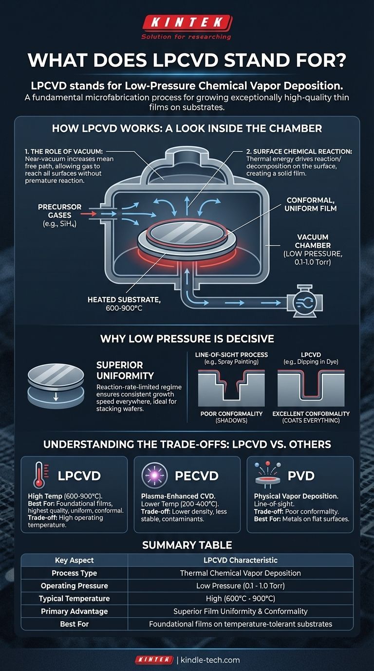
LPCVD stands for Low-Pressure Chemical Vapor Deposition. It is a fundamental process used in microfabrication and semiconductor manufacturing to grow exceptionally high-quality thin films of material onto a substrate, such as a silicon wafer. This method is a cornerstone for building the intricate, layered structures that form modern microelectronic devices.
The term "Low-Pressure" is not just a detail; it is the defining characteristic that enables the process. By operating in a near-vacuum, LPCVD creates films with superior uniformity and an unmatched ability to conformally coat complex three-dimensional structures.
How LPCVD Works: A Look Inside the Chamber
LPCVD is a thermal process that relies on chemical reactions occurring directly on the surface of a heated substrate. Understanding the key elements reveals why it is so effective.
The Role of Vacuum (Low Pressure)
The process takes place inside a sealed chamber where the pressure is reduced to a near-vacuum (typically 0.1 to 1.0 Torr). This low pressure is critical because it significantly increases the mean free path of the gas molecules—the average distance a molecule travels before colliding with another.
This allows precursor gases to travel throughout the chamber and reach all substrate surfaces without reacting prematurely in the gas phase.
The Chemical Reaction on the Surface
Once the chamber is under vacuum, one or more reactive precursor gases are introduced. The substrates are heated to high temperatures, often between 600°C and 900°C.
This thermal energy provides the activation energy needed for the precursor gases to react or decompose upon contact with the hot surface, leaving behind a solid, stable thin film. For example, silane gas (SiH₄) is used to deposit a film of pure silicon.
The Result: A High-Quality Film
Because the reaction is driven by surface temperature and not by gas-phase transport, the film grows at a very controlled and predictable rate. This results in films that are highly uniform across the entire substrate and conformal, meaning they coat the vertical sidewalls of trenches just as thickly as they coat the flat top surfaces.
Why Low Pressure is the Decisive Factor
The low-pressure environment directly leads to the two most important advantages of LPCVD: uniformity and conformality. These properties are often non-negotiable for high-performance device manufacturing.
Achieving Superior Uniformity
At low pressures, the deposition rate is limited by the speed of the chemical reaction on the surface, not by the rate at which gas molecules can travel to the surface (mass transport).
This reaction-rate-limited regime ensures that the film grows at the same speed everywhere, regardless of minor variations in gas flow. This allows dozens or even hundreds of wafers to be stacked vertically in a furnace and coated simultaneously with excellent uniformity.
Gaining Excellent Conformality
The long mean free path of the gas molecules ensures they can diffuse deep into complex, high-aspect-ratio trenches and structures before reacting.
Think of it like spray painting (a line-of-sight process that leaves "shadows") versus dipping an object in a vat of dye (which coats all surfaces evenly). LPCVD acts like the dye, providing a perfect, conformal coating that is essential for insulating or conducting over complex topographies.
Understanding the Trade-offs: LPCVD vs. Other Methods
LPCVD is a workhorse, but it's not the only tool available. Its primary trade-off is its high operating temperature, which dictates where in a manufacturing flow it can be used.
LPCVD vs. PECVD: The Temperature Dilemma
Plasma-Enhanced CVD (PECVD) uses an electromagnetic field to create a plasma, which provides the energy for the chemical reaction instead of high heat. This allows PECVD to operate at much lower temperatures (e.g., 200-400°C).
However, PECVD films often have lower density, higher internal stress, and incorporate contaminants like hydrogen from the precursor gases. LPCVD films are generally purer and more stable.
LPCVD vs. PVD: Chemical vs. Physical Deposition
Physical Vapor Deposition (PVD) methods like sputtering use physical force (e.g., ion bombardment) to knock atoms from a target and deposit them onto a substrate.
PVD is a line-of-sight process, resulting in poor conformality. It's excellent for depositing metals on flat surfaces but cannot effectively coat the sidewalls of deep trenches, a task where LPCVD excels.
Making the Right Choice for Your Goal
The choice between LPCVD and other deposition techniques is driven entirely by the material requirements and the thermal constraints of the manufacturing step.
- If your primary focus is the highest structural quality and conformality: LPCVD is the unmatched standard for foundational films like polysilicon and silicon nitride that define transistor gates and provide robust insulation.
- If your primary focus is depositing a film at low temperatures: PECVD is essential when depositing layers on top of materials that cannot withstand high heat, such as aluminum or copper interconnects.
- If your primary focus is depositing a metal film quickly: PVD (sputtering) is the go-to method for creating the metallic layers used for wiring and contacts.
Ultimately, understanding the physics behind each deposition method empowers you to select the precise process needed to build reliable and high-performance devices.
Summary Table:
| Key Aspect | LPCVD Characteristic |
|---|---|
| Process Type | Thermal Chemical Vapor Deposition |
| Operating Pressure | Low Pressure (0.1 - 1.0 Torr) |
| Typical Temperature | High (600°C - 900°C) |
| Primary Advantage | Superior Film Uniformity & Conformality |
| Best For | Foundational films (e.g., polysilicon, silicon nitride) on temperature-tolerant substrates |
Ready to integrate precise LPCVD processes into your microfabrication workflow? KINTEK specializes in providing high-quality lab equipment and consumables for semiconductor manufacturing and advanced material science. Our expertise ensures you have the reliable tools needed to achieve superior film quality and device performance. Contact our experts today to discuss your specific laboratory needs and how we can support your innovation.
Visual Guide
Related Products
- Chemical Vapor Deposition CVD Equipment System Chamber Slide PECVD Tube Furnace with Liquid Gasifier PECVD Machine
- Microwave Plasma Chemical Vapor Deposition MPCVD Machine System Reactor for Lab and Diamond Growth
- Inclined Rotary Plasma Enhanced Chemical Vapor Deposition PECVD Equipment Tube Furnace Machine
- Customer Made Versatile CVD Tube Furnace Chemical Vapor Deposition Chamber System Equipment
- Split Chamber CVD Tube Furnace with Vacuum Station Chemical Vapor Deposition System Equipment Machine
People Also Ask
- What are the advantages of chemical vapor deposition? Achieve Superior Thin Films for Your Lab
- What is the chemical vapor deposition growth process? Build Superior Thin Films from the Atom Up
- Why is Chemical Vapor Deposition (CVD) equipment uniquely suited for constructing hierarchical superhydrophobic structures?
- What are the processes of vapor phase deposition? Understand CVD vs. PVD for Superior Thin Films
- How are carbon nanotubes grown? Master Scalable Production with Chemical Vapor Deposition