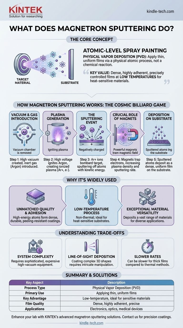
At its core, magnetron sputtering is a physical vapor deposition (PVD) method used to apply exceptionally thin and uniform films of one material onto another surface. Think of it as a form of highly controlled, atomic-level spray painting. This process is not a chemical reaction but a physical one, where atoms from a source material (the "target") are ejected and deposited onto a substrate to create a high-performance coating.
The true value of magnetron sputtering lies in its ability to produce dense, highly adherent, and precisely controlled thin films at low temperatures. This makes it indispensable for creating advanced coatings on heat-sensitive materials like plastics and electronics, something thermal-based methods cannot easily achieve.
How Magnetron Sputtering Works
To understand what magnetron sputtering does, it's essential to understand its mechanism. The process occurs inside a vacuum chamber and can be broken down into a few key steps. It's best visualized as a game of cosmic billiard balls.
Step 1: Creating a Vacuum and Introducing a Gas
First, all air is removed from a chamber to create a high vacuum. This ensures the purity of the film by removing any contaminants. Then, a small amount of an inert gas, typically Argon, is introduced into the chamber.
Step 2: Generating a Plasma
A high negative voltage is applied to the source material, known as the target. This voltage ignites the Argon gas, stripping electrons from the Argon atoms and turning the gas into a plasma—a glowing, ionized gas made of positive Argon ions and free electrons.
Step 3: The Sputtering Event
The positively charged Argon ions are powerfully attracted to the negatively charged target. They accelerate and collide with the target's surface with significant kinetic energy. This bombardment is like an atomic-scale sandblasting, knocking individual atoms or molecules off the target. These ejected particles are now "sputtered."
Step 4: The Crucial Role of the Magnets
This is what separates magnetron sputtering from other forms. Powerful magnets are placed behind the target. These magnets trap the free electrons from the plasma in a magnetic field directly in front of the target.
This electron trap dramatically increases the probability that electrons will collide with and ionize more Argon gas atoms. The result is a much denser, more intense plasma concentrated where it's needed most, leading to a significantly higher rate of sputtering and deposition.
Step 5: Deposition onto the Substrate
The sputtered atoms from the target travel through the vacuum chamber and land on the object being coated (the substrate). Because these atoms arrive with high energy, they form a very dense, uniform, and strongly bonded thin film on the substrate's surface.
Why This Process Is So Widely Used
The unique characteristics of the sputtering process give it several key advantages that have made it a cornerstone of modern manufacturing.
Unmatched Film Quality and Adhesion
The high energy of the sputtered atoms ensures they embed themselves firmly onto the substrate. This creates coatings that are incredibly dense, durable, and resistant to peeling or flaking compared to many other coating methods.
A Low-Temperature Process
Because the process relies on kinetic energy (bombardment) rather than heat, it is considered a "non-thermal" technology. This is a critical advantage, as it allows for the coating of heat-sensitive materials like plastics, finished electronic components, and advanced polymers without causing damage.
Exceptional Material Versatility
Magnetron sputtering can be used to deposit a vast range of materials. This includes metals, alloys, ceramics, and other insulating compounds, making it suitable for an enormous variety of applications, from simple metallic finishes to complex multi-layer optical stacks.
Understanding the Trade-offs
No technology is without its limitations. Being a trusted advisor means acknowledging the situations where magnetron sputtering might not be the best fit.
System Complexity and Cost
Sputtering systems require a significant investment. The need for high-vacuum chambers, sophisticated power supplies, and strong magnetic arrays makes the equipment more complex and expensive than simpler methods like thermal evaporation.
Line-of-Sight Deposition
Much like spray painting, sputtering is a line-of-sight process. The sputtered material travels in a relatively straight line from the target to the substrate. Coating complex, three-dimensional shapes with uniform thickness requires intricate substrate rotation and manipulation, which adds to the process complexity.
Potentially Slower Deposition Rates
While the magnetron significantly boosts sputtering rates compared to older diode methods, it can still be a slower process than high-rate thermal methods for depositing thick films. Its strength lies in precision and quality, not necessarily raw speed.
How to Apply This to Your Project
Your choice to use magnetron sputtering should be driven by the specific properties your final product requires.
- If your primary focus is performance and precision: Magnetron sputtering is ideal for creating dense, pure, and highly adherent thin films, especially when electrical, optical, or wear-resistant properties are critical.
- If your primary focus is coating heat-sensitive materials: This process is one of the best choices available, as its non-thermal nature protects substrates like polymers, integrated circuits, and medical devices from heat damage.
- If your primary focus is high-volume, simple coatings: For applications where film density is less critical and the substrate is robust, you should evaluate if faster and less complex methods like thermal evaporation could meet your cost and throughput goals.
By understanding its core principles, you can leverage magnetron sputtering to engineer materials with properties that were previously unachievable.
Summary Table:
| Key Aspect | Description |
|---|---|
| Process Type | Physical Vapor Deposition (PVD) |
| Primary Use | Applying thin, uniform films of materials onto substrates |
| Key Advantage | Low-temperature process ideal for heat-sensitive materials |
| Film Quality | Dense, highly adherent, and precisely controlled coatings |
| Common Applications | Electronics, optics, medical devices, durable tool coatings |
Ready to enhance your lab's capabilities with precision coatings? KINTEK specializes in advanced lab equipment and consumables, including magnetron sputtering solutions tailored for research and production needs. Whether you're working with sensitive electronics, optical components, or innovative materials, our expertise ensures you achieve the high-quality, durable thin films your projects demand. Contact us today to discuss how our solutions can drive your success!
Visual Guide
Related Products
- Spark Plasma Sintering Furnace SPS Furnace
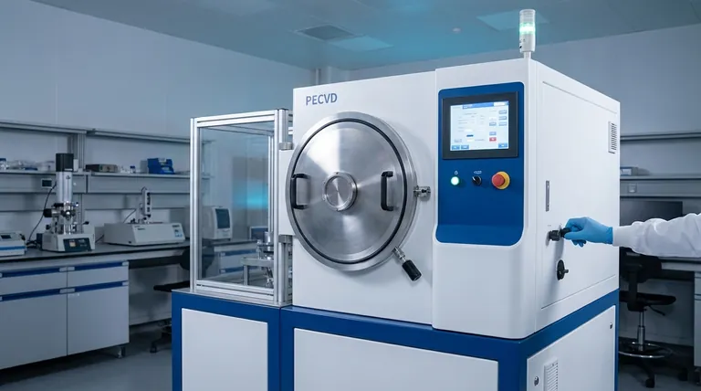
- RF PECVD System Radio Frequency Plasma-Enhanced Chemical Vapor Deposition RF PECVD
People Also Ask
- What technical advantages does a Spark Plasma Sintering (SPS) furnace offer for LZP ceramics? Enhance Ionic Conductivity
- What are the advantages of CAMI/SPS for W-Cu composite preparation? Reduce cycles from hours to seconds.
- What is the process fundamentals of spark plasma sintering? Achieve Rapid, High-Density Material Consolidation
- What is the pressure for spark plasma sintering? A Guide to Optimizing SPS Parameters
- What is the difference between spark plasma sintering and flash sintering? A Guide to Advanced Sintering Methods

