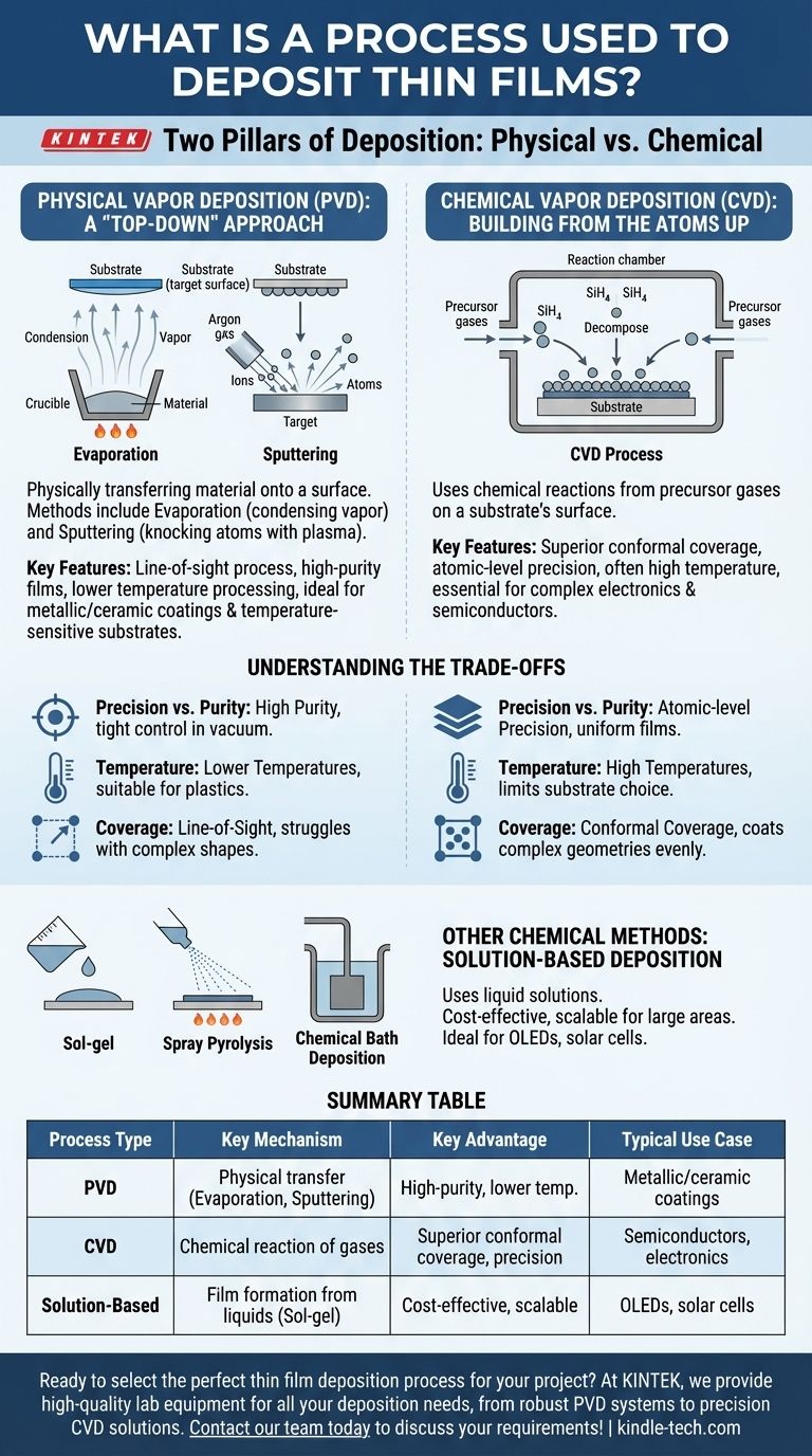
The primary processes for depositing thin films fall into two major categories: Physical Vapor Deposition (PVD) and Chemical Vapor Deposition (CVD). PVD involves physically transferring a material onto a surface, for example by boiling it and letting it condense (evaporation) or by knocking atoms off a target with plasma (sputtering). CVD uses chemical reactions from precursor gases on a substrate’s surface to grow the film atom by atom.
The core challenge in thin film deposition is moving material from a source to a substrate with precise control. The choice between a physical process (like sandblasting at an atomic scale) and a chemical process (like building a structure brick by brick) depends entirely on the required film purity, precision, and the material being used.
The Two Pillars of Deposition: Physical vs. Chemical
At the highest level, all deposition techniques are designed to create a functional layer of material, often just a few atoms or molecules thick. The fundamental difference lies in how that material travels from its source to the target surface, known as the substrate.
Physical Vapor Deposition (PVD): A "Top-Down" Approach
PVD methods take a solid or liquid source material and transform it into a vapor, which then condenses on the substrate as a thin film. This is fundamentally a line-of-sight process.
The two most common PVD techniques are evaporation and sputtering.
Evaporation involves heating a source material in a vacuum until it turns into a gas. This gas then travels and deposits onto the cooler substrate, forming a pure, solid film.
Sputtering is a more energetic process. Here, a target of the desired material is bombarded with high-energy ions (often from a gas like argon). This collision physically knocks atoms off the target, which then deposit onto the substrate.
Chemical Vapor Deposition (CVD): Building from the Atoms Up
CVD is a fundamentally different approach that relies on chemical reactions, not just physical transfer. It is the dominant method used in the semiconductor industry for its exceptional precision.
In a CVD process, the substrate is placed in a reaction chamber and exposed to one or more volatile precursor gases. These gases react or decompose on the substrate's surface, leaving behind a solid material to form the desired film.
Other Chemical Methods: Solution-Based Deposition
Beyond CVD, other chemical methods use liquid solutions to create films. These are often simpler and can be more cost-effective for certain applications.
Techniques like sol-gel, spray pyrolysis, and chemical bath deposition involve applying a liquid chemical solution to the substrate. The film is then formed as the liquid is dried, heated, or chemically reacted.
Understanding the Trade-offs
Choosing between PVD and CVD isn't about which is "better," but which is right for the job. Each approach comes with a distinct set of advantages and limitations.
Precision vs. Purity
CVD is unparalleled in its ability to create uniform, conformal films with atomic-level thickness control. This precision is why it's essential for manufacturing complex, layered semiconductor devices.
PVD methods, particularly sputtering, are celebrated for producing films of extremely high purity, as the process can be tightly controlled in a high-vacuum environment without complex chemical precursors.
Temperature and Substrate Sensitivity
CVD processes often require high temperatures to induce the necessary chemical reactions on the substrate surface. This can limit their use with materials that are sensitive to heat.
Many PVD processes, especially sputtering, can be performed at much lower temperatures. This makes them suitable for depositing films on plastics, polymers, and other temperature-sensitive substrates.
Line-of-Sight vs. Conformal Coverage
Because PVD is a physical, line-of-sight process, it can struggle to evenly coat complex, three-dimensional shapes with sharp corners or deep trenches.
CVD, by contrast, excels at creating conformal coatings. Because the precursor gases can flow around complex geometries, the resulting film grows uniformly over the entire exposed surface.
Making the Right Choice for Your Goal
The optimal deposition technique is dictated by your application's specific requirements for material properties, precision, and cost.
- If your primary focus is high-purity metallic or ceramic coatings: PVD methods like sputtering are an excellent, highly controllable choice.
- If your primary focus is atomic-level precision for complex electronics: CVD is the industry standard for its ability to grow flawless, conformal layers.
- If your primary focus is large-area or flexible devices like OLEDs or solar cells: Simpler, solution-based chemical methods can offer a scalable and cost-effective pathway.
Understanding the fundamental difference between physical transfer and chemical reaction empowers you to select the process that best aligns with your material and performance goals.
Summary Table:
| Process Type | Key Mechanism | Key Advantage | Typical Use Case |
|---|---|---|---|
| Physical Vapor Deposition (PVD) | Physical transfer of material (e.g., evaporation, sputtering) | High-purity films, lower temperature processing | Metallic/ceramic coatings, temperature-sensitive substrates |
| Chemical Vapor Deposition (CVD) | Chemical reaction of gases on a substrate surface | Superior conformal coverage, atomic-level precision | Semiconductors, complex electronics |
| Solution-Based Chemical Methods | Film formation from liquid precursors (e.g., sol-gel) | Cost-effective for large areas, scalable | OLEDs, solar cells, large-area coatings |
Ready to select the perfect thin film deposition process for your project? The right equipment is critical for achieving the desired film purity, precision, and performance. At KINTEK, we specialize in providing high-quality lab equipment and consumables for all your deposition needs, from robust PVD systems to precision CVD solutions. Let our experts help you optimize your process. Contact our team today to discuss your specific application requirements!
Visual Guide
Related Products
- CVD Diamond Dressing Tools for Precision Applications
- Multi Heating Zones CVD Tube Furnace Machine Chemical Vapor Deposition Chamber System Equipment
- CVD Diamond Domes for Industrial and Scientific Applications
- CVD Diamond for Thermal Management Applications
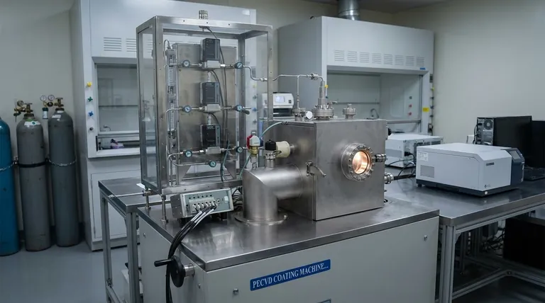
- Chemical Vapor Deposition CVD Equipment System Chamber Slide PECVD Tube Furnace with Liquid Gasifier PECVD Machine
People Also Ask
- What is CVD diamond? The Ultimate Guide to Lab-Grown Diamonds and Their Uses
- What are the raw materials for CVD diamonds? A seed, a gas, and the science of crystal growth.
- What color diamonds are CVD? Understanding the Process from Brown Tint to Colorless Beauty
- How do you identify a CVD diamond? The Definitive Guide to Lab-Grown Diamond Verification
- How long does it take to make synthetic diamonds? Discover the 6-8 Week Science Behind Lab-Grown Gems


