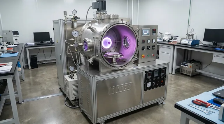
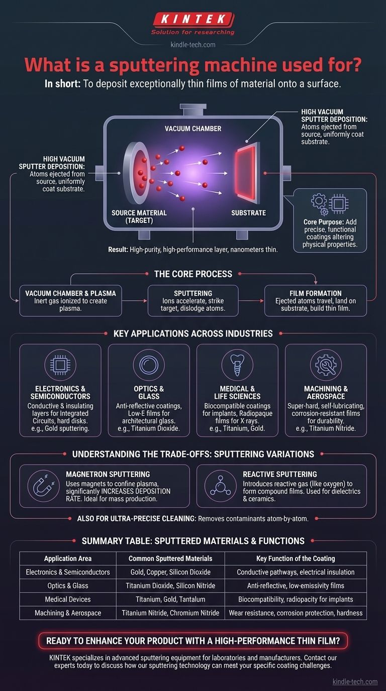
In short, a sputtering machine is used to deposit exceptionally thin films of material onto a surface. This process, known as sputter deposition, operates in a high vacuum by ejecting atoms from a source material (a "target") and uniformly coating them onto a component (a "substrate"). The result is a high-purity, high-performance layer that can be as thin as a few nanometers.
Sputtering is a foundational technology for modern manufacturing. Its core purpose is to add precise, functional coatings that alter a material's physical properties, enabling everything from the circuitry in your phone to the anti-reflective coating on your glasses.
The Core Process: How Sputter Deposition Works
Sputter deposition is a highly controlled technique belonging to a category known as Physical Vapor Deposition (PVD). The goal is always to transfer material atom-by-atom from a source to a target.
The Basic Mechanism
The process begins by placing a target, made of the desired coating material, and a substrate, the object to be coated, into a vacuum chamber. An inert gas (like argon) is introduced and ionized, creating a plasma. These ions are then accelerated into the target, striking it with enough force to dislodge or "sputter" individual atoms.
Forming the Thin Film
These ejected atoms travel through the vacuum chamber and land on the substrate, gradually building up a thin, uniform, and highly pure film. Because this happens in a vacuum, there are no contaminants to interfere with the coating's quality.
Why It's a Go-To Method
Sputtering is valued for its precision and versatility. It can be used with a vast range of materials, including metals, alloys, and ceramics, and provides excellent control over the film's thickness, density, and adhesion to the substrate.
Key Applications Across Industries
The ability to create these precise, functional films makes sputtering essential in numerous high-tech fields. It's not just about aesthetics; it's about adding critical performance characteristics.
Electronics and Semiconductors
This is one of sputtering's largest applications. It is used to deposit conductive and insulating layers during the manufacturing of integrated circuits, transistors, and computer hard disks. Gold sputtering, for example, is used to coat circuit panels due to gold's excellent conductivity.
Optics and Glass
Sputtering creates functional optical films with special properties. This includes anti-reflective coatings on lenses, translucent films, and low-emissivity (Low-E) films on architectural glass that reflect heat while letting light pass through.
Medical and Life Sciences
In medicine, sputtering is used to apply biocompatible coatings to implants. It can also create radiopaque films on devices, making them visible in X-rays. For research, gold sputtering is used to coat tissue samples so they can be viewed under a powerful scanning electron microscope.
Machining and Aerospace
For industrial applications, sputtering creates surface functional films that enhance durability. These include super-hard films to protect cutting tools, self-lubricating films for moving parts, and corrosion-resistant coatings to protect sensitive materials in harsh environments.
Understanding the Trade-offs: Sputtering Variations
Not all sputtering is the same. Different techniques are employed to achieve specific outcomes, often by modifying the basic process to improve speed or create different types of materials.
Magnetron Sputtering
This is the most common industrial method. By using powerful magnets behind the target, the plasma is confined near the target's surface. This dramatically increases the rate of deposition, making the process faster and more efficient for mass production.
Reactive Sputtering
This technique is used to create compound films. It works by introducing a reactive gas (like oxygen or nitrogen) into the vacuum chamber along with the inert gas. The sputtered metal atoms react with this gas to form a new compound, such as a dielectric or a ceramic, on the substrate. This is widely used for creating resistors and insulators in semiconductors.
Uses Beyond Coating
While deposition is its primary function, sputtering is also used as an ultra-precise cleaning method. By lightly sputtering a surface, contaminants can be removed atom-by-atom to prepare a high-purity surface for further analysis or processing.
How to Apply This to Your Goal
The specific sputtering technique used is determined entirely by the desired outcome for the final product.
- If your primary focus is high-volume electronics manufacturing: Magnetron sputtering is the industry standard for depositing conductive and insulating layers efficiently.
- If your primary focus is creating specialized optical surfaces: Sputtering offers the precision needed for multi-layer anti-reflective, reflective, or light-filtering coatings.
- If your primary focus is enhancing the durability of mechanical parts: Sputtering is used to apply super-hard, anti-corrosion, or self-lubricating films that extend component life.
- If your primary focus is developing advanced medical devices: Sputtering provides biocompatible and radiopaque coatings essential for implants and diagnostic tools.
Ultimately, sputtering is the enabling technology that imparts high-performance properties to the surfaces of countless modern products.
Summary Table:
| Application Area | Common Sputtered Materials | Key Function of the Coating |
|---|---|---|
| Electronics & Semiconductors | Gold, Copper, Silicon Dioxide | Conductive pathways, electrical insulation |
| Optics & Glass | Titanium Dioxide, Silicon Nitride | Anti-reflective, low-emissivity (Low-E) films |
| Medical Devices | Titanium, Gold, Tantalum | Biocompatibility, radiopacity for implants |
| Machining & Aerospace | Titanium Nitride, Chromium Nitride | Wear resistance, corrosion protection, hardness |
Ready to enhance your product with a high-performance thin film?
KINTEK specializes in advanced sputtering equipment and consumables for laboratories and manufacturers. Whether you are developing next-generation semiconductors, durable medical implants, or precision optical components, our solutions deliver the uniformity, purity, and control your R&D and production demand.
Contact our experts today to discuss how our sputtering technology can meet your specific coating challenges.
Visual Guide
Related Products
- Single Punch Manual Tablet Press Machine TDP Tablet Punching Machine
- Lab Scale Rotary Single Punch Tablet Press Machine TDP Tablet Punching Machine
- Single Punch Electric Tablet Press Machine TDP Tablet Punching Machine
- Twin Screw Extruder Plastic Granulation Machine
- Single Punch Tablet Press Machine and Mass Production Rotary Tablet Punching Machine for TDP
People Also Ask
- What is a tablet punching machine called? Choosing the Right Press for Your Production Scale
- What are the different parts of a single punch tablet machine? The Core Components Explained
- What is the use of single punch tablet press? For Precise R&D and Small-Batch Tablet Production
- What is a tablet punch? The Precision Tool Shaping Your Tablet Manufacturing
- What are advantages of single punch tablet press machine? Maximize R&D Efficiency with Minimal Material