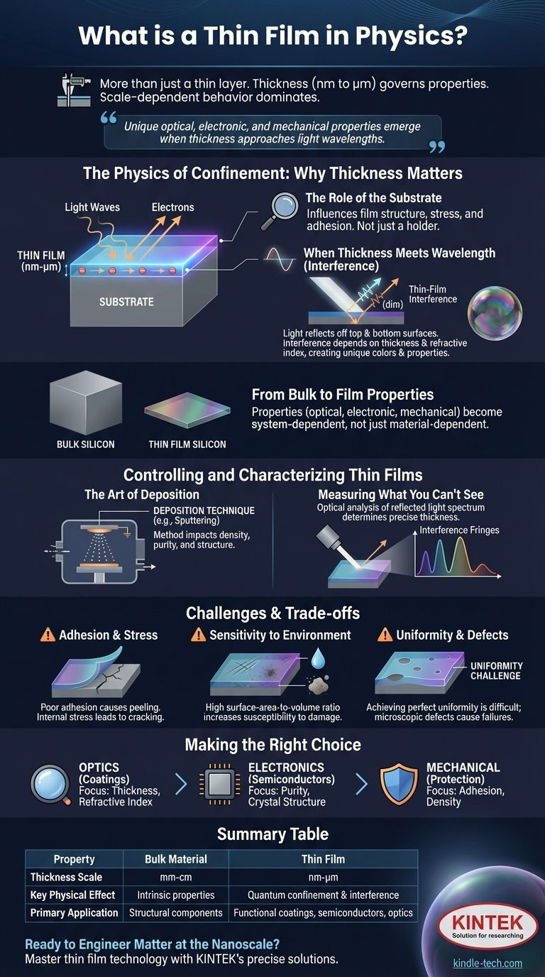
In physics, a thin film is not just a thin layer of material. It is a layer deposited onto a substrate with a thickness so small—ranging from a few nanometers to several micrometers—that its physical properties are fundamentally governed by its dimensions. This scale-dependent behavior is what separates a thin film from the same material in its bulk form.
A thin film's defining characteristic is its scale. When a material's thickness approaches the wavelength of light or other critical physical lengths, quantum and wave-interference effects begin to dominate, creating unique optical, electronic, and mechanical properties that do not exist in the bulk material.
The Physics of Confinement: Why Thickness Changes Everything
The unique nature of a thin film arises because its two large-area surfaces are incredibly close together. This proximity forces physical phenomena, like light waves or electrons, to interact with the material in a highly constrained way.
The Role of the Substrate
A thin film does not exist in isolation; it is grown on a substrate. This underlying material is not merely a passive holder.
The substrate's crystal structure, temperature, and surface chemistry directly influence the film's own structure, stress, and adhesion, fundamentally shaping its final characteristics.
When Thickness Meets Wavelength
The most intuitive unique property of thin films is their interaction with light. This is driven by thin-film interference.
When light hits a film, some reflects off the top surface, and some enters the film and reflects off the bottom surface (at the film-substrate interface). These two reflected waves then interfere with each other.
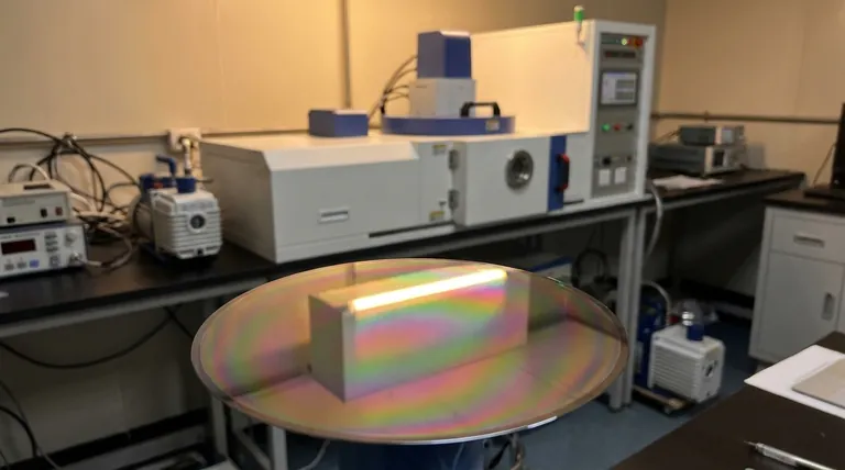
Depending on the film's thickness and its refractive index, this interference can be constructive (amplifying certain colors) or destructive (canceling others out). This is the principle behind the iridescent colors of a soap bubble or an anti-reflection coating on eyeglasses.
From Bulk Properties to Film Properties
A block of silicon is opaque and grey, but a thin film of silicon can be transparent or appear colored. This demonstrates how properties are no longer inherent to the material alone.
Instead, the film's characteristics—be they optical, electronic, or mechanical—become a property of the entire system: the film material, its thickness, the substrate, and the deposition method used to create it.
Controlling and Characterizing Thin Films
Because a film's properties are so dependent on its structure, the methods of creation and measurement are critical disciplines.
The Art of Deposition
The deposition technique—the method used to apply the film to the substrate—is a crucial factor.
Techniques like sputtering, evaporation, or chemical vapor deposition have an enormous impact on the film's density, purity, internal stress, and crystalline structure. The choice of method is dictated by the desired application.
Measuring What You Can't See
Precisely measuring the thickness of a transparent film is often done optically. By analyzing the spectrum of light reflected from the film, scientists can observe the peaks and valleys created by interference.
Using the known refractive index of the film material, the number and position of these interference fringes allow for a highly accurate calculation of the film's thickness.
Defining its Purpose
The unique properties engineered into thin films enable a vast range of applications. They can be designed to meet specific photonic, electronic, mechanical, or chemical requirements.
For example, an optical film might be designed for anti-reflection, a mechanical film for scratch resistance, and an electronic film to act as a semiconductor in a transistor.
Understanding the Trade-offs and Challenges
While powerful, thin film technology comes with inherent engineering challenges that are not present in bulk materials.
The Problem of Adhesion and Stress
A film is only as good as its bond to the substrate. Poor adhesion can cause the film to peel or flake off, rendering it useless.
Furthermore, internal stress built up during the deposition process can cause the film to crack or deform, compromising its integrity.
Sensitivity to Environment
By their very nature, thin films have a massive surface-area-to-volume ratio. This makes them far more susceptible to damage from scratches, chemical corrosion, and environmental degradation than a solid block of the same material.
Uniformity and Defects
Achieving a perfectly uniform thickness across an entire substrate, especially a large one, is a significant manufacturing challenge.
Even microscopic defects, such as pinholes or dust particles, can cause a catastrophic failure in an electronic circuit or create a weak point in a protective coating.
Making the Right Choice for Your Goal
When evaluating a thin film for an application, your primary focus determines which property is most critical.
- If your primary focus is optics (e.g., coatings): Your chief concern will be precise control over thickness and refractive index to manage light interference.
- If your primary focus is electronics (e.g., semiconductors): You must prioritize material purity, crystal structure, and the quality of the interface with the substrate.
- If your primary focus is mechanical protection (e.g., hard coatings): Adhesion to the substrate and film density will be your most important metrics.
Ultimately, mastering thin film technology is about engineering matter at a scale where fundamental physical laws create entirely new possibilities.
Summary Table:
| Property | Bulk Material | Thin Film |
|---|---|---|
| Thickness Scale | Millimeters to centimeters | Nanometers to micrometers |
| Key Physical Effect | Intrinsic material properties | Quantum confinement & interference |
| Primary Application | Structural components | Functional coatings, semiconductors, optics |
Ready to Engineer Matter at the Nanoscale?
Mastering thin film technology requires precise control over deposition and characterization. KINTEK specializes in high-quality lab equipment and consumables for all your thin film research and production needs—from sputtering systems to thickness measurement tools.
Contact our experts today to discuss how our solutions can help you achieve superior film uniformity, adhesion, and performance for your specific application in optics, electronics, or protective coatings.
Visual Guide
Related Products
- Aluminized Ceramic Evaporation Boat for Thin Film Deposition
- Tungsten Evaporation Boat for Thin Film Deposition
- Electron Beam Evaporation Coating Oxygen-Free Copper Crucible and Evaporation Boat
- Molybdenum Tungsten Tantalum Evaporation Boat for High Temperature Applications
- Aluminum-Plastic Flexible Packaging Film for Lithium Battery Packaging
People Also Ask
- What is thin film deposition? Unlock Advanced Surface Engineering for Your Materials
- What are thin films deposited by evaporation? A Guide to High-Purity Coating
- What is the source of evaporation for thin film? Choosing Between Thermal and E-Beam Methods
- Why is an alumina boat and Ti3AlC2 powder bed necessary for Ti2AlC sintering? Protect MAX Phase Purity
- Why are high-purity ceramic boats used for lignin activation? Ensure Purity & Thermal Stability


