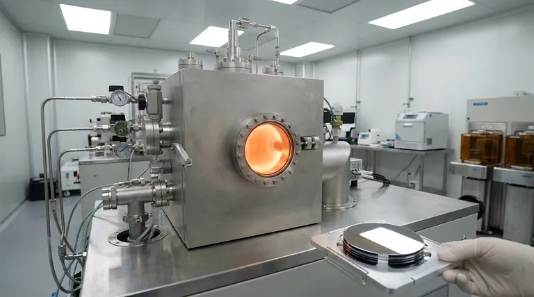
A classic example of chemical vapor deposition (CVD) is the process used to create the ultrapure polysilicon and silicon dioxide layers that form the foundation of microchips and solar panels. In this process, a precursor gas like silane (SiH₄) is introduced into a high-temperature vacuum chamber, where it chemically reacts and decomposes. This deposits a solid, highly pure, and perfectly uniform thin film of silicon onto a substrate, such as a silicon wafer.
Chemical vapor deposition is not a single process, but a versatile family of techniques for building thin films or nanostructures from the "bottom-up." By carefully controlling gaseous chemical reactions, CVD allows us to construct materials with exceptional purity and structural precision, making it a cornerstone of modern electronics and material science.
How a CVD Process Fundamentally Works
At its core, every CVD process involves transforming a gas-phase chemical (a "precursor") into a solid material on a surface (a "substrate"). This method allows for atomic-level control over the film's growth.
The Key Ingredients and Steps
- Precursor Introduction: A volatile precursor gas, containing the atoms you want to deposit, is fed into a reaction chamber. For silicon dioxide (SiO₂), this might be a gas like TEOS (tetraethyl orthosilicate).
- Energy Application: Energy is supplied to the chamber to initiate a chemical reaction. This is the main differentiating factor between CVD types. It can be high heat (Thermal CVD) or an energized plasma field (Plasma-Enhanced CVD).
- Chemical Reaction: The energy breaks down the precursor molecules. The desired atoms are freed and adsorb onto the substrate's surface.
- Film Deposition & Byproduct Removal: A stable, solid thin film forms on the substrate. Unwanted chemical byproducts from the reaction are removed from the chamber by a vacuum or gas flow system.
The Many Forms of Chemical Vapor Deposition
The term "CVD" refers to a category of processes, each optimized for different materials, temperatures, and applications. The primary distinction is how the reaction is powered.
Thermal CVD
This is the most traditional form, relying solely on high temperatures (often several hundred to over a thousand degrees Celsius) to break down the precursor gas.
- Low-Pressure CVD (LPCVD): Performed in a vacuum, this method produces films of outstanding purity and uniformity. It is widely used for depositing polysilicon and silicon dioxide in the semiconductor industry.
- Atmospheric-Pressure CVD (APCVD): This process is faster and simpler as it doesn't require a vacuum, but the film quality is generally lower.
Plasma-Enhanced CVD (PECVD)
Instead of relying only on high heat, PECVD uses an ionized gas, or plasma, to energize the precursor gases. This allows deposition to occur at much lower temperatures, making it suitable for substrates that cannot withstand the heat of thermal CVD.
Other Specialized Methods
- Metalorganic CVD (MOCVD): Uses specialized metalorganic precursors to create complex semiconductor materials, such as gallium nitride (GaN) for LEDs and advanced electronics.
- Aerosol-Assisted CVD (AACVD): Dissolves the precursor in a solvent, creates an aerosol, and injects it into the chamber. This technique broadens the range of usable precursor materials.
Understanding the Advantages and Trade-offs
CVD is an indispensable manufacturing technique, but choosing it requires understanding its benefits and inherent constraints.
The Key Advantages
- High Purity: Because the precursors are highly refined gases and the process occurs in a controlled chamber, the resulting films are exceptionally pure.
- Uniform Coating: CVD is a non-line-of-sight process. The gas flows around objects, allowing for a perfectly uniform coating on complex, three-dimensional shapes.
- Versatility: A vast range of materials can be deposited, including semiconductors (silicon), dielectrics (silicon dioxide), metals (tungsten), and ceramics (titanium nitride).
- Excellent Adhesion: The chemical bonding process results in films that adhere extremely well to the substrate.
Common Considerations and Pitfalls
- Hazardous Precursors: The gases used in CVD processes can be highly toxic, flammable, or corrosive, requiring significant safety infrastructure.
- High Temperatures: Traditional thermal CVD methods can damage temperature-sensitive substrates, such as plastics or certain electronic components. This is a primary reason for using PECVD.
- Equipment Complexity: CVD reactors, particularly those using high vacuums and plasma generation, are complex and expensive to purchase and maintain.
How to Apply This to Your Project
Your choice of CVD method is dictated entirely by your material, substrate, and desired film quality.
- If your primary focus is creating high-purity semiconductor layers: LPCVD and PECVD are the industry standards for depositing materials like polysilicon and silicon dioxide on wafers.
- If your primary focus is coating a temperature-sensitive material: PECVD is the superior choice because it uses plasma energy, allowing for deposition at significantly lower temperatures.
- If your primary focus is achieving a uniform protective coating on complex parts: The non-line-of-sight nature of CVD makes it ideal for uniformly hardening cutting tools or preventing corrosion on intricate components.
- If your primary focus is rapid deposition with simpler equipment: APCVD offers a faster, lower-cost alternative when the absolute highest purity and uniformity are not required.
By understanding the principles of CVD, you can select the precise technique to construct the high-performance materials your project demands.
Summary Table:
| CVD Method | Primary Use | Key Characteristic |
|---|---|---|
| Thermal CVD (LPCVD) | High-purity semiconductor layers (e.g., polysilicon) | High temperature, excellent purity & uniformity |
| Plasma-Enhanced CVD (PECVD) | Coating temperature-sensitive materials (e.g., plastics) | Lower temperature, uses plasma energy |
| Metalorganic CVD (MOCVD) | Complex semiconductors (e.g., GaN for LEDs) | Uses specialized metalorganic precursors |
| Atmospheric-Pressure CVD (APCVD) | Rapid deposition with simpler equipment | Faster process, no vacuum required |
Ready to build high-purity, uniform thin films for your lab or production needs?
KINTEK specializes in providing advanced lab equipment and consumables for precise chemical vapor deposition processes. Whether you're developing microchips, solar panels, or specialized coatings, our expertise ensures you achieve exceptional material purity and structural precision.
Contact our CVD experts today to discuss how our solutions can enhance your research and manufacturing outcomes!
Visual Guide

Related Products
- CVD Diamond Dressing Tools for Precision Applications
- Multi Heating Zones CVD Tube Furnace Machine Chemical Vapor Deposition Chamber System Equipment
- CVD Diamond Domes for Industrial and Scientific Applications
- CVD Diamond for Thermal Management Applications
- Chemical Vapor Deposition CVD Equipment System Chamber Slide PECVD Tube Furnace with Liquid Gasifier PECVD Machine
People Also Ask
- How do you identify a CVD diamond? The Definitive Guide to Lab-Grown Diamond Verification
- Can CVD diamonds change color? No, their color is permanent and stable.
- How long does it take to make synthetic diamonds? Discover the 6-8 Week Science Behind Lab-Grown Gems
- Does the chemical vapor deposition be used for diamonds? Yes, for Growing High-Purity Lab Diamonds
- What is chemical vapor deposition of diamond? Grow High-Purity Diamonds Atom-by-Atom


