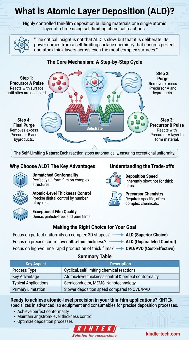
In essence, atomic layer deposition (ALD) is a highly controlled thin-film deposition technique that builds materials one single atomic layer at a time. It uses a sequence of self-limiting chemical reactions with gas-phase materials, called precursors, to deposit exceptionally uniform and conformal films with angstrom-level precision. This cycle is repeated until the desired total film thickness is achieved.
The critical insight is not that ALD is slow, but that it is deliberate. Its power comes from a self-limiting surface chemistry that ensures perfect, one-atom-thick layers across even the most complex surfaces, a level of control other deposition methods cannot achieve.
The Core Mechanism: A Step-by-Step Cycle
Unlike processes that deposit material continuously, ALD is a cyclical process. Each cycle deposits a single monolayer of material and consists of four distinct steps, which are the key to its precision.
Step 1: The First Precursor Pulse
A gas-phase precursor chemical (Precursor A) is introduced into the process chamber. This precursor reacts with the surface of the substrate until all available reactive sites are occupied.
Step 2: The Purge
Excess, unreacted Precursor A and any gaseous byproducts are removed from the chamber, typically with an inert gas like nitrogen or argon. This step is critical to prevent unwanted reactions in the gas phase.
Step 3: The Second Precursor Pulse
A second precursor (Precursor B), often a reactant like water or ozone, is pulsed into the chamber. It reacts specifically with the layer of Precursor A that is already bound to the surface, forming the desired material.
Step 4: The Final Purge
Again, the chamber is purged with an inert gas to remove any unreacted Precursor B and the byproducts from the second reaction. This completes one full cycle, leaving behind a single, uniform layer of the target material.
The Self-Limiting Nature
The foundation of ALD's precision is its self-limiting nature. Each precursor reaction stops automatically once all available surface sites are consumed. You cannot deposit more than one monolayer per half-cycle, no matter how much extra precursor you introduce. This is what guarantees the exceptional film uniformity.
Why Choose ALD? The Key Advantages
The unique mechanism of ALD provides benefits that are essential for advanced manufacturing, particularly in semiconductors and nanotechnology.
Unmatched Conformality
Because the gas precursors can reach every part of a surface, ALD can coat highly complex, three-dimensional structures with a perfectly uniform film. The thickness of the film will be the same on the top, sides, and deep inside trenches.
Atomic-Level Thickness Control
The final film thickness is determined simply by the number of cycles performed. If one cycle deposits 1 angstrom of material, 100 cycles will deposit a film that is precisely 100 angstroms thick. This digital control is unparalleled.
Exceptional Film Quality
The layer-by-layer growth process results in films that are incredibly dense, pinhole-free, and pure. The purging steps ensure that contaminants and byproducts are efficiently removed between each layer, leading to high-quality material.
Understanding the Trade-offs
Despite its powerful advantages, ALD is not the solution for every application. Its primary limitation is a direct consequence of its strength.
Deposition Speed
Building a film one atomic layer at a time is inherently slow. For applications requiring very thick films (microns, not nanometers), the time required can be prohibitive, making other methods like Chemical Vapor Deposition (CVD) more practical.
Precursor Chemistry
ALD relies on highly specific precursor chemicals that have the right reactivity and volatility. Developing and sourcing these specialized precursors can be complex and expensive, especially for new or exotic materials.
Making the Right Choice for Your Goal
Selecting a deposition technique depends entirely on the requirements of your final product.
- If your primary focus is perfect uniformity on complex 3D shapes (like coating a MEMS device or a transistor gate): ALD is the industry standard and the superior choice.
- If your primary focus is precise control over ultra-thin film thickness (from a few angstroms to tens of nanometers): The digital, cyclic nature of ALD provides unparalleled control.
- If your primary focus is high-volume, rapid production of relatively thick, simple films: A faster method like Physical Vapor Deposition (PVD) or Chemical Vapor Deposition (CVD) is likely more cost-effective.
Ultimately, ALD provides a level of deliberate, atomic-scale construction that other techniques simply cannot match.
Summary Table:
| Key Aspect | Description |
|---|---|
| Process Type | Cyclical, self-limiting chemical reactions |
| Key Advantage | Atomic-level thickness control & perfect conformality |
| Typical Applications | Semiconductor manufacturing, MEMS devices, nanotechnology |
| Primary Limitation | Slower deposition speed compared to CVD/PVD |
Ready to achieve atomic-level precision in your thin-film applications?
KINTEK specializes in advanced lab equipment and consumables for precise deposition processes. Our expertise in ALD technology can help you:
- Achieve perfect conformality on complex 3D structures
- Maintain angstrom-level thickness control
- Optimize your deposition processes for superior film quality
Contact our experts today to discuss how our ALD solutions can enhance your research and manufacturing outcomes.
Visual Guide
Related Products
- RF PECVD System Radio Frequency Plasma-Enhanced Chemical Vapor Deposition RF PECVD
- Chemical Vapor Deposition CVD Equipment System Chamber Slide PECVD Tube Furnace with Liquid Gasifier PECVD Machine
- HFCVD Machine System Equipment for Drawing Die Nano-Diamond Coating
- Customer Made Versatile CVD Tube Furnace Chemical Vapor Deposition Chamber System Equipment
- 915MHz MPCVD Diamond Machine Microwave Plasma Chemical Vapor Deposition System Reactor
People Also Ask
- What is the role of RF-PECVD in VFG preparation? Mastering Vertical Growth and Surface Functionality
- How does Radio Frequency Enhanced Plasma Chemical Vapour Deposition (RF-PECVD) work? Learn the Core Principles
- What is plasma enhanced chemical vapour deposition PECVD used for? Enable Low-Temp Thin Films for Electronics & Solar
- How does plasma enhance CVD? Unlock Low-Temperature, High-Quality Film Deposition
- What is plasma chemical vapor deposition? A Low-Temperature Thin Film Coating Solution


