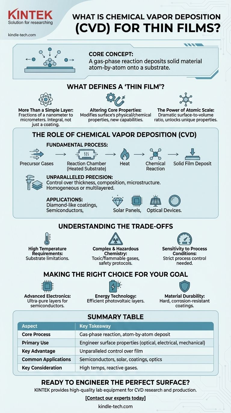
At its core, Chemical Vapor Deposition (CVD) is a highly precise manufacturing process used to grow an ultra-thin layer of solid material onto a surface. It works by introducing specific gases, known as precursors, into a reaction chamber where they decompose and deposit a high-performance film, molecule by molecule, onto a target object or substrate. This method is fundamental to creating the specialized surfaces that power modern electronics, energy systems, and advanced materials.
The crucial insight is that CVD is not merely a coating technique like painting; it is a bottom-up construction method. It allows us to build entirely new material surfaces with unique optical, electrical, or mechanical properties that the underlying object does not possess on its own.
What Defines a "Thin Film"?
More Than a Simple Layer
A thin film is a layer of material ranging from fractions of a nanometer (a single layer of atoms) to several micrometers in thickness.
Unlike a simple coating, a thin film becomes an integral part of the object, fundamentally changing the properties of its surface.
Altering Core Properties
The primary purpose of a thin film is to modify the physical and chemical properties of a surface without altering the bulk material underneath.
This allows an object to gain new capabilities, such as corrosion resistance, electrical conductivity, or heat resistance, while retaining its original structural integrity.
The Power of Atomic Scale
When materials are reduced to thin-film dimensions, their surface-to-volume ratio increases dramatically.
This change in scale unlocks unique material properties that are not present in the bulk form, enabling innovations across countless industries.
The Role of Chemical Vapor Deposition
The Fundamental Process
CVD can be thought of as a controlled chemical reaction in the gas phase. Precursor gases are introduced into a chamber containing the substrate, which is typically heated.
The heat provides the energy needed to trigger a reaction, causing a solid material to form and deposit uniformly onto the substrate surface, creating the thin film.
Unparalleled Precision and Control
The CVD process offers exceptional control over the film’s thickness, composition, and microstructure.
Engineers can create films that are perfectly homogeneous, composed of a single crystalline structure, or designed as complex multilayered structures to achieve specific performance goals.
Applications Across Industries
This precision makes CVD essential for a vast range of applications, from producing diamond-like carbon films for wear resistance to creating the delicate layers in semiconductors.
It is used to manufacture everything from solar panels and microchips to optical devices and protective coatings on aerospace components.
Understanding the Trade-offs
High Temperature Requirements
Many CVD processes require very high temperatures to initiate the necessary chemical reactions. This can limit the types of materials that can be used as substrates, as some may deform or melt under such conditions.
Complex and Hazardous Chemistry
The precursor gases used in CVD can be highly toxic, flammable, or corrosive. This necessitates sophisticated safety protocols, specialized handling equipment, and complex waste management systems, which can increase operational costs.
Sensitivity to Process Conditions
The quality of the final film is extremely sensitive to process parameters like temperature, pressure, and gas flow rates. Even minor deviations can lead to defects, making strict process control absolutely critical for achieving consistent and reliable results.
Making the Right Choice for Your Goal
The application of thin films via CVD is driven by the specific property you need to engineer.
- If your primary focus is advanced electronics: CVD is the foundational process for building the ultra-pure, precisely structured layers required for semiconductors and thin film transistors.
- If your primary focus is energy technology: This method is critical for manufacturing the efficient photovoltaic layers in thin film solar cells and the high-performance components of modern batteries.
- If your primary focus is material durability: CVD creates exceptionally hard, corrosion-resistant, and heat-resistant coatings that protect critical components in harsh aerospace and industrial environments.
Ultimately, Chemical Vapor Deposition empowers us to engineer the high-performance surfaces that define the capabilities of our most advanced technologies.
Summary Table:
| Aspect | Key Takeaway |
|---|---|
| Core Process | A gas-phase reaction that deposits solid material atom-by-atom onto a substrate. |
| Primary Use | To engineer a surface with new optical, electrical, or mechanical properties. |
| Key Advantage | Unparalleled control over film thickness, composition, and structure. |
| Common Applications | Semiconductors, solar panels, wear-resistant coatings, and optical devices. |
| Key Consideration | Often requires high temperatures and careful handling of reactive gases. |
Ready to engineer the perfect surface for your application?
Chemical Vapor Deposition is a powerful tool for creating specialized thin films. Whether your lab is focused on developing advanced electronics, next-generation energy solutions, or ultra-durable materials, having the right equipment is critical.
KINTEK specializes in providing high-quality lab equipment and consumables for all your thin-film research and production needs. Our expertise can help you achieve the precise control and reliable results that CVD demands.
Contact our experts today to discuss how we can support your laboratory's specific goals with the right CVD solutions.
Visual Guide
Related Products
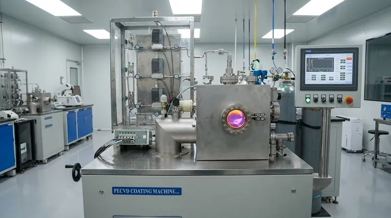
- Chemical Vapor Deposition CVD Equipment System Chamber Slide PECVD Tube Furnace with Liquid Gasifier PECVD Machine
- Microwave Plasma Chemical Vapor Deposition MPCVD Machine System Reactor for Lab and Diamond Growth
- 915MHz MPCVD Diamond Machine Microwave Plasma Chemical Vapor Deposition System Reactor
- Customer Made Versatile CVD Tube Furnace Chemical Vapor Deposition Chamber System Equipment
- HFCVD Machine System Equipment for Drawing Die Nano-Diamond Coating
People Also Ask
- What is plasma enhanced chemical vapor deposition PECVD equipment? A Guide to Low-Temperature Thin Film Deposition
- Why is Chemical Vapor Deposition (CVD) equipment uniquely suited for constructing hierarchical superhydrophobic structures?
- What happens during deposition chemistry? Building Thin Films from Gaseous Precursors
- How are carbon nanotubes grown? Master Scalable Production with Chemical Vapor Deposition
- What are the advantages of chemical vapor deposition? Achieve Superior Thin Films for Your Lab


