In advanced manufacturing, Chemical Vapor Deposition (CVD) is a process for depositing a high-purity, high-performance solid material from a gas or vapor onto a surface. It is not a coating in the traditional sense of painting or spraying; rather, it "grows" an entirely new solid layer on a target object, known as a substrate. This method is fundamental to producing key components in industries ranging from semiconductors to synthetic diamonds.
CVD is fundamentally a chemical process, not a physical one. It uses energy—typically heat—to trigger a chemical reaction in a gas, causing a new, ultra-pure solid layer to grow directly onto a target surface, often atom by atom.
How CVD Works: The Core Principles
Understanding CVD requires visualizing it as a controlled chemical reaction occurring on a surface. The entire process is meticulously managed inside a specialized chamber.
The Vacuum Chamber Environment
First, the object to be coated (the substrate) is placed inside a sealed vacuum chamber. Removing all other gases is critical to prevent contamination and ensure the purity of the final deposited material.
Introducing the Reactants (Precursors)
Next, one or more volatile gases, known as precursors, are introduced into the chamber. These precursor gases contain the specific atoms needed to create the desired solid film (e.g., a carbon-containing gas to create a diamond film).
Activating the Chemical Reaction
Energy, most often in the form of very high heat, is applied to the substrate. This energy breaks down the precursor gas molecules, triggering chemical reactions.
Deposition and Growth
The reactive chemical species then deposit onto the heated substrate, forming a stable, solid, and thin film. This film grows layer by layer, resulting in a highly uniform and dense material that is chemically bonded to the surface.
Managing By-products
The chemical reactions often produce volatile by-products. These are unwanted gases that are continuously removed from the chamber by a gas-flow or vacuum system, keeping the reaction environment clean.
Key Applications of CVD
The precision of CVD makes it indispensable for creating materials that would be difficult or impossible to produce otherwise.
Semiconductor Manufacturing
This is one of the largest applications of CVD. It is used to deposit various ultra-thin films of insulating, conducting, or semiconducting materials onto silicon wafers. These layers are the building blocks of the microprocessors and memory chips that power all modern electronics.
Creating High-Purity Synthetic Diamonds
CVD is a primary method for creating lab-grown diamonds. By introducing a carbon-containing gas into a chamber with a small diamond "seed," the process builds new diamond crystals, atom by atom. These are used in jewelry and for industrial applications like cutting tools.
Protective and Functional Coatings
The process is used to apply extremely hard, corrosion-resistant, and wear-resistant coatings onto machine tools, engine components, and other industrial parts. It is also used to create specialized optical coatings, such as anti-reflective layers on lenses.
Understanding the Trade-offs
While powerful, CVD is a complex and resource-intensive technique. Its selection requires careful consideration of its inherent challenges.
High Equipment and Operational Costs
CVD reactors, vacuum systems, and the associated gas handling equipment are expensive to acquire and maintain. The process often consumes significant amounts of energy.
Complex Process Control
The final quality of the deposited film is extremely sensitive to variables like temperature, pressure, and gas flow rates. Achieving consistent, high-quality results requires sophisticated control systems and deep process expertise.
Hazardous Precursor Materials
The precursor gases used in CVD can be highly toxic, flammable, or corrosive. This necessitates strict safety protocols, specialized handling equipment, and waste management systems, adding to operational complexity.
Making the Right Choice for Your Goal
Deciding if CVD is the correct manufacturing approach depends entirely on your end goal and technical requirements.
- If your primary focus is atomic-level precision and purity: CVD is the definitive choice for applications like microelectronics, where flawless, uniform layers are non-negotiable.
- If your primary focus is creating exceptionally hard or pure materials: CVD is a leading method for growing synthetic diamonds or applying high-performance wear-resistant films.
- If your primary focus is cost-sensitive, large-scale coating: You must carefully evaluate if CVD's high performance justifies its cost compared to alternatives like Physical Vapor Deposition (PVD).
Ultimately, choosing CVD is a commitment to precision and performance at the atomic scale.
Summary Table:
| Key Aspect | Description |
|---|---|
| Process Type | Chemical reaction to grow a solid layer from a gas/vapor. |
| Primary Use | High-purity, high-performance thin films and materials. |
| Key Industries | Semiconductor manufacturing, synthetic diamonds, protective coatings. |
| Main Advantage | Atomic-level precision and exceptional material purity. |
| Main Challenge | High equipment cost and complex process control. |
Need high-purity materials or precision coatings for your lab? KINTEK specializes in advanced lab equipment and consumables, including solutions for processes like CVD. Our expertise can help you achieve the material performance and reliability your research demands. Contact our experts today to discuss your specific laboratory needs!
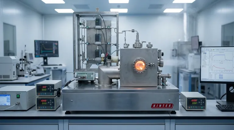
Visual Guide

Related Products
- Chemical Vapor Deposition CVD Equipment System Chamber Slide PECVD Tube Furnace with Liquid Gasifier PECVD Machine
- Customer Made Versatile CVD Tube Furnace Chemical Vapor Deposition Chamber System Equipment
- Microwave Plasma Chemical Vapor Deposition MPCVD Machine System Reactor for Lab and Diamond Growth
- 915MHz MPCVD Diamond Machine Microwave Plasma Chemical Vapor Deposition System Reactor
- Custom CVD Diamond Coating for Lab Applications
People Also Ask
- What happens during deposition chemistry? Building Thin Films from Gaseous Precursors
- How are carbon nanotubes grown? Master Scalable Production with Chemical Vapor Deposition
- How expensive is chemical vapor deposition? Understanding the True Cost of High-Performance Coating
- What types of substrates are used in CVD to facilitate graphene films? Optimize Graphene Growth with the Right Catalyst
- What are the advantages of chemical vapor deposition? Achieve Superior Thin Films for Your Lab


