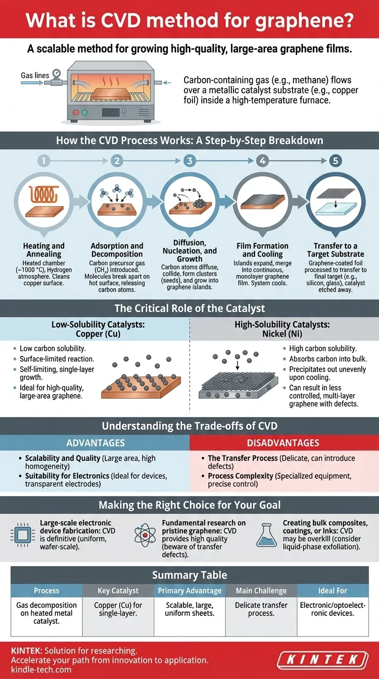
In essence, Chemical Vapor Deposition (CVD) is a scalable synthesis method for growing high-quality, large-area graphene films. The process involves flowing a carbon-containing gas, such as methane, over a metallic catalyst substrate like copper foil inside a high-temperature furnace. The heat causes the gas to decompose, depositing carbon atoms onto the metal surface, where they self-assemble into a continuous, single-atom-thick sheet of graphene.
CVD is the most important method for producing graphene on an industrial scale. It solves the primary challenge of creating large, uniform sheets required for real-world electronic and optical applications, moving graphene from a lab curiosity to a viable engineering material.
How the CVD Process Works: A Step-by-Step Breakdown
To understand why CVD is so crucial, it’s helpful to break down the process into its core stages. The entire procedure occurs within a controlled vacuum chamber or furnace.
Step 1: Heating and Annealing
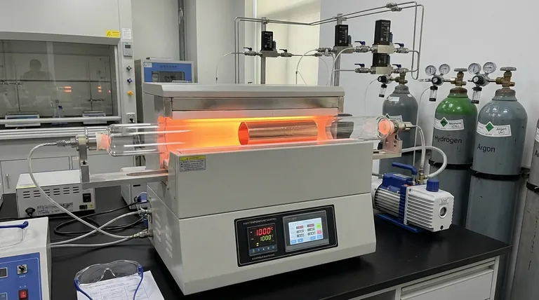
First, a catalytic metal substrate, most commonly a thin foil of copper (Cu), is placed in the reactor. The chamber is heated to a high temperature, typically around 1000 °C, in a hydrogen atmosphere. This step cleans the copper surface and prepares it for growth.
Step 2: Adsorption and Decomposition
A small amount of a carbon precursor gas, like methane (CH₄), is introduced into the chamber. At these high temperatures, the precursor gas molecules adsorb, or "stick," to the hot copper surface and break apart, releasing individual carbon atoms.
Step 3: Diffusion, Nucleation, and Growth
These freed carbon atoms diffuse, or "skate," across the metal surface. They eventually collide to form small, stable carbon clusters, which act as nucleation sites or "seeds." Subsequent carbon atoms preferentially attach to the edges of these seeds, causing them to grow into larger islands of graphene.
Step 4: Film Formation and Cooling
As the deposition continues, these individual graphene islands expand and merge, eventually forming a continuous, monolayer graphene film that covers the entire surface of the copper foil. Once the growth is complete, the system is cooled down.
Step 5: Transfer to a Target Substrate
The graphene is now on the metal catalyst, but it's needed on a different substrate (like silicon or glass) for most applications. The graphene-coated foil is carefully processed to transfer the graphene sheet to the final target, after which the original metal catalyst is etched away.
The Critical Role of the Catalyst
The choice of metal catalyst is not arbitrary; it fundamentally dictates the growth mechanism and the quality of the final graphene film.
Low-Solubility Catalysts: Copper (Cu)
Copper has a very low carbon solubility, meaning it cannot absorb many carbon atoms. This forces the carbon atoms to remain on the surface.
This surface-limited reaction is largely self-limiting, stopping once the surface is covered with a single layer. This makes copper the ideal catalyst for producing high-quality, large-area, single-layer graphene.
High-Solubility Catalysts: Nickel (Ni)
Nickel has a high carbon solubility. At high temperatures, it absorbs a significant amount of carbon into its bulk, like a sponge soaking up water.
Upon cooling, the solubility drops, and the absorbed carbon precipitates back out onto the surface. This can result in less controlled, multi-layer graphene with more defects, as the carbon comes out of the bulk metal unevenly.
Understanding the Trade-offs of CVD
While powerful, the CVD method is not without its challenges. A balanced understanding is key to its effective use.
Advantage: Scalability and Quality
CVD is the most promising method for producing graphene with a large surface area and high homogeneity. It provides excellent control over the number of layers (especially with copper), yielding high-purity, uniform films suitable for mass production.
Advantage: Suitability for Electronics
The ability to create large, continuous sheets is precisely what is needed for fabricating electronic and optoelectronic devices. This makes CVD graphene ideal for applications like transparent electrodes, photodetectors, and next-generation transistors.
Disadvantage: The Transfer Process
The necessity of transferring the graphene film from the metal catalyst to a functional substrate is the process's primary weakness. This step is delicate and can easily introduce wrinkles, tears, contamination, and other defects that degrade the graphene's exceptional properties.
Disadvantage: Process Complexity
While relatively inexpensive compared to some niche academic methods, CVD is not a simple benchtop process. It requires specialized vacuum furnaces, high temperatures, and precise control over gas flow rates, making the initial equipment investment significant.
Making the Right Choice for Your Goal
Selecting a graphene synthesis method depends entirely on your end-use application. CVD excels in specific domains where its unique advantages are paramount.
- If your primary focus is large-scale electronic device fabrication: CVD is the definitive method due to its ability to produce the uniform, wafer-scale films required for industrial integration.
- If your primary focus is fundamental research on pristine graphene: CVD provides high-quality material, but be aware that the transfer step is a critical variable that can introduce performance-limiting defects.
- If your primary focus is creating bulk composites, coatings, or inks: CVD may be overkill; other methods like liquid-phase exfoliation might provide sufficient material more cost-effectively.
Understanding the principles of CVD is essential for anyone looking to harness graphene's potential for technology, as it represents the most viable bridge from laboratory discovery to functional innovation.
Summary Table:
| Aspect | Details |
|---|---|
| Process | Gas decomposition on a heated metal catalyst substrate (e.g., copper). |
| Key Catalyst | Copper (Cu) for self-limiting, single-layer growth. |
| Primary Advantage | Scalable production of large, uniform, high-quality sheets. |
| Main Challenge | Delicate transfer process can introduce defects. |
| Ideal For | Electronic/optoelectronic devices like transparent electrodes and transistors. |
Ready to integrate high-quality graphene into your research or product development?
KINTEK specializes in providing the advanced lab equipment and expert support needed for cutting-edge material synthesis like CVD. Our solutions help you achieve the precise control required for growing uniform graphene films, accelerating your path from innovation to application.
Contact our experts today to discuss how we can support your laboratory's specific needs.
Visual Guide
Related Products
- HFCVD Machine System Equipment for Drawing Die Nano-Diamond Coating
- Chemical Vapor Deposition CVD Equipment System Chamber Slide PECVD Tube Furnace with Liquid Gasifier PECVD Machine
- Customer Made Versatile CVD Tube Furnace Chemical Vapor Deposition Chamber System Equipment
- Microwave Plasma Chemical Vapor Deposition MPCVD Machine System Reactor for Lab and Diamond Growth
- 915MHz MPCVD Diamond Machine Microwave Plasma Chemical Vapor Deposition System Reactor
People Also Ask
- What is the function of tungsten filaments in HFCVD? Powering Diamond Film Synthesis with Thermal Excitation
- What types of substrates are used in CVD to facilitate graphene films? Optimize Graphene Growth with the Right Catalyst
- What are the advantages of chemical vapor deposition? Achieve Superior Thin Films for Your Lab
- What is the full form of HFCVD? A Guide to Hot Filament Chemical Vapor Deposition
- What is the chemical vapor deposition growth process? Build Superior Thin Films from the Atom Up


