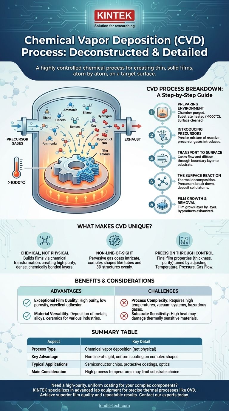
In essence, Chemical Vapor Deposition (CVD) is a highly controlled process for creating thin, solid films on a surface. It works by introducing reactive gases (precursors) into a heated chamber, where they undergo a chemical reaction on a target object (the substrate), depositing a new layer of material atom by atom. This method is fundamental to manufacturing everything from computer chips to durable protective coatings.
The true power of CVD lies not just in its ability to deposit a film, but in its chemical nature. Unlike physical methods, CVD "grows" a high-purity, uniform layer that can conform to complex shapes, making it a cornerstone technology for advanced electronics and durable materials.
Deconstructing the CVD Process: A Step-by-Step Breakdown
At its core, CVD is a sophisticated and precise sequence of events. Each step is critical for building a high-quality film with the desired properties.
Step 1: Preparing the Environment
Before any deposition can occur, the stage must be set perfectly. This involves placing the substrate (the object to be coated) inside a reaction chamber.
The chamber is then purged of any residual gases, and the substrate is heated, often to temperatures over 1000°C. This intense heat cleans the substrate surface and provides the thermal energy needed to drive the upcoming chemical reactions.
Step 2: Introducing the Precursors
Once the chamber is hot and clean, a carefully measured mixture of precursor gases is introduced. These gases contain the atoms that will ultimately form the final film.
The flow rate, concentration, and ratio of these gases are controlled with extreme precision, as they directly influence the chemistry of the deposition.
Step 3: Transport to the Surface
The precursor gases flow through the chamber and diffuse across a stationary boundary layer of gas that forms just above the heated substrate.
Successfully transporting the reactive species through this layer to the substrate surface is crucial for achieving a uniform coating.
Step 4: The Surface Reaction
This is the heart of the CVD process. When the precursor gases are adsorbed (attach) onto the hot substrate surface, the thermal energy triggers a chemical reaction.
This reaction, often a form of thermal decomposition, breaks the precursor molecules apart, leaving behind the desired solid atoms which bond to the surface.
Step 5: Film Growth and Byproduct Removal
As the solid atoms deposit, they form a thin, dense, and highly pure film on the substrate. The film grows layer by layer, creating a coating with a controlled thickness and structure.
Meanwhile, any unwanted gaseous byproducts from the chemical reaction are transported away from the substrate and exhausted from the chamber.
What Makes CVD Unique?
CVD is not the only way to create a thin film, but its underlying principles give it distinct and powerful advantages.
It's a Chemical, Not Physical, Process
Unlike methods like sputtering, which physically knock atoms from a target onto a substrate, CVD builds the film through a chemical transformation. This allows for the creation of highly pure, dense, and even single-crystal films that are chemically bonded to the substrate.
Non-Line-of-Sight Deposition
Because the deposition is driven by a pervasive gas, CVD is not a "line-of-sight" process. The precursor gases can flow into and coat the surfaces of incredibly complex shapes, including the insides of tubes or intricate three-dimensional structures.
Precision Through Control
The final properties of the film—such as its thickness, purity, and crystalline structure—are not left to chance. They are directly tuned by adjusting the key process parameters: temperature, pressure, and gas flow rates. This gives engineers immense control over the final material.
Understanding the Advantages and Trade-offs
No process is perfect for every application. Understanding the strengths and inherent challenges of CVD is key to using it effectively.
Advantage: Exceptional Film Quality
CVD is renowned for producing films with high purity and very low porosity. The resulting coatings are dense, durable, and adhere exceptionally well to the substrate.
Advantage: Material Versatility
A wide array of materials can be deposited using CVD, including pure metals, complex alloys, and hard ceramics. This makes the process suitable for a diverse range of industries, from optics to aerospace.
Potential Challenge: Process Complexity
The use of high temperatures, vacuum systems, and reactive (sometimes hazardous) precursor gases means CVD equipment is complex and requires stringent process control and safety protocols.
Potential Challenge: Substrate Sensitivity
The high temperatures required for many CVD processes can damage or warp thermally sensitive substrates. This can limit the types of materials that can be successfully coated.
When is CVD the Right Choice?
Base your decision on the specific, non-negotiable requirements of your final product.
- If your primary focus is coating complex, non-flat surfaces: CVD is superior because its gas-phase nature allows it to deposit uniformly on intricate geometries where line-of-sight methods would fail.
- If your primary focus is achieving the highest material purity and density: CVD's chemical reaction process excels at creating films with very few impurities or voids, which is critical for high-performance electronics and optics.
- If your primary focus is coating temperature-sensitive materials: You must carefully verify if the standard CVD process temperature is compatible with your substrate, or investigate lower-temperature variants like Plasma-Enhanced CVD (PECVD).
Ultimately, mastering CVD is about precisely controlling chemistry and environmental conditions to build superior materials from the ground up.
Summary Table:
| Aspect | Key Detail |
|---|---|
| Process Type | Chemical vapor deposition (not physical) |
| Key Advantage | Non-line-of-sight, uniform coating on complex shapes |
| Typical Applications | Semiconductor chips, protective coatings, optics |
| Main Consideration | High process temperatures may limit substrate choice |
Need a high-purity, uniform coating for your complex components? KINTEK specializes in advanced lab equipment and consumables for precise thermal processes like CVD. Our solutions help laboratories achieve superior film quality and repeatable results. Contact our experts today via our contact form to discuss how we can support your specific material deposition challenges.
Visual Guide
Related Products
- Customer Made Versatile CVD Tube Furnace Chemical Vapor Deposition Chamber System Equipment
- Chemical Vapor Deposition CVD Equipment System Chamber Slide PECVD Tube Furnace with Liquid Gasifier PECVD Machine
- CVD Diamond for Thermal Management Applications
- Custom CVD Diamond Coating for Lab Applications
- HFCVD Machine System Equipment for Drawing Die Nano-Diamond Coating
People Also Ask
- What is the function of a tube furnace in CVD SiC synthesis? Achieving Ultra-Pure Silicon Carbide Powders
- How does a CVD tube furnace inhibit the sintering of silver supports? Boost Membrane Durability and Performance
- What is the difference between hot wall CVD and cold wall CVD? Choose the Right System for Your Process
- What is the function of a high-temperature CVD tube furnace in 3D graphene foam prep? Master 3D Nanomaterial Growth
- What is a CVD furnace? The Ultimate Guide to Precision Thin-Film Coating


